Imagine a world without a Printed Circuit board? Quite unimaginable, the tangled wires would have been all over the places. A Smartphone holds around 11000 centimeters of wire inside it, to connect a speaker, Antenna, GPS, battery, Wi-Fi, sensors, and many more components into a single device.
But where are these wires? Are they invisible like the “Invisible Man”?

Nah, thanks to PCB, which is a multilayered labyrinth of hundreds of copper wires.
What are RF Circuits, and how an RF circuits work?
RF stands for radio frequency, is a form of energy in the modification of time-dependent electromagnetic fields. It propagates readily in a vacuum or solid-state through circuit boards or coaxial cables. PCB circuits which propagates electromagnetic wave between 1 Megahertz and 3 Gigahertz classified as RF circuits. Anything above 3 Gigahertz up to 30 Gigahertz considered as Microwave PCB circuits. RF circuit boards find their usage in many upcoming technologies, such as smartphones, sensors, and in many of the military applications.
Several critical factors influence the RF circuit board design.
1) Bypassing/Decoupling
2) Trace length
3) Interfaces and Ground plane
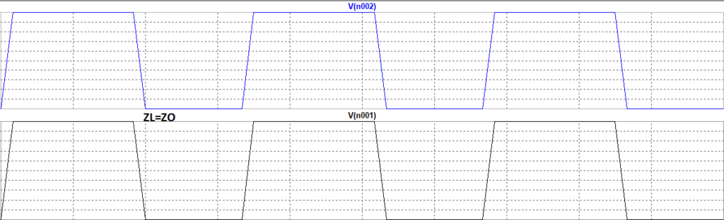
When we work with real-world power supply, it’s not perfect since they don’t have infinite output impedance.
Any SPICE simulation tools, it depicts a perfect line, but that’s not the reality shown in the figure below.
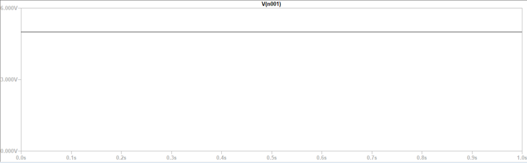
Figure1: Ideal Spice Simulation
Why decoupling capacitors must be considered for RF circuit design?
In a high-speed PCB design, any active components such as operational amplifiers, microprocessors, or high-density BGA, there are many decoupling capacitors. The decoupling capacitor helps in eliminating most of the noise the circuit encounters.
Any real-world circuit that deals with high-speed signals or sensitive low-level signals things turn complicated. The realistic approximation of a capacitor is an RLC circuit, a real-world capacitor, has parasitic inductance, and resistance. Since it is a series RLC circuit, the frequency at which the capacitor no longer acts as a capacitor becomes an inductor and no longer decouples the circuit.
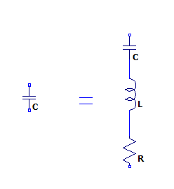
Figure 2: Realistic approximation of a capacitor
Circuits that cover a wide range of frequency must have multiple decoupling capacitors. When design engineers work on high-speed PCB design, bypassing/decoupling forms a crucial factor. Most of the suppliers or manufacturers recommend out particular bypass requirements with any specific design requirements based on the datasheets.
How to determine the trace length?
When we work on SPICE simulation tools, we think wires as an interconnect points, that’s not true when we are working with high-speed signals, then all the interconnections have to be treated as a transmission line. Engineers must find out the highest frequency their design will be dealing with if the traces exceed about 1/10 of the wavelength of that frequency, then engineers must model the interconnect as the transmission line.
Absolute frequency of the waveform may not be the critical aspect, but the fastest rise time will determine the circuit’s quickest frequency. Let us consider a 20 Hertz square wave, and the rise time is about 200ns, frequency is inverse of the rise time we get 25 MHZ.
How quickly signals move through the circuitry, is determined by the speed of light divided by the square root of the relative permittivity of the material.
Rise time= 200ns
Highest frequency=1/Rise time=25 MHZ.
To determine the speed of the wave (V)
V=Speed of Light/Sqrt (Relative Permittivity)
Relative Permittivity for FR-4 Material is 4.
V=3×10^8/Sqrt (4) =1.5×10^8
Wavelength=Speed of wave/ Frequency= 1.5×10^8/25 x 10^6= 6 meters.
1/10th of the wavelength will be 60 centimeters, which would be approximately around 2 feet. If the traces are longer than 2 feet, then interconnects must be considered as transmission lines, which would interfere with the propagation of the signal.
How impedance match affect the RF circuit design?
The next important factor a design engineer needs to ponder is the impedance match. To deliver the power efficiently across the connection, or wire, the impedance must match. The figure below depicts impedance mismatch in high-speed PCB design.
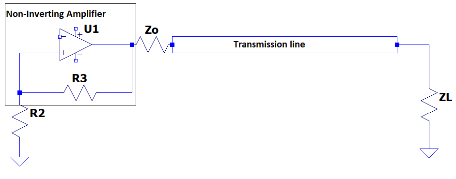
Figure3: Characteristic impedance mismatch
Due to impedance mismatch, the signal gets distorted. The rate of distortion is directly proportional to the change in impedance. When the signal enters the transmission line, if the impedance matches, then the output signal matches the input signal. The signal passing through an Op-amp and if there is an impedance mismatch, the reflection will create the distortion, this is one of the crucial factors for the RF circuits and RS-485 communication protocols.
For the RF circuit design, the next crucial aspect is the importance of grounding. For high-speed circuit design, you cannot treat ground as an infinite sink of current due to a parasitic inductance, capacitance, and resistance we need to consider.
Ground plane forms a crucial factor for the RF circuit designs, bigger the ground plane lesser the inductance and resistance, and helps to shield the circuits from EMI. EMI, defined as an electronic emission considered as noise signals, can be in the form of electrical noise or radiation noise emitted by the device or the other devices nearby.
Let us consider a real-time example to understand how EMI can impact the High-speed circuit operation. During the airplane takeoff/landing, the cabin crew requests us to switch off our mobile phones and laptops. Have you ever thought about why they ask us to do that?
The radiation emitted by mobile phones and laptops will disturb the airplanes high frequency operating communication equipment. Communication between the airplane and radar interrupted due to the noise generated through smartphones and laptops. Any design engineer’s goal is to reduce the EMI to meet the requirements given by the Federal Communication Commission or the CISPR. On a PCB, we don’t want to use the trace as ground. Ideally, we want the ground plane to be bigger and flatter, which helps to reduce the parasitic inductance.
Importance of grounding arrangement in RF circuit design
There are different grounding arrangements
1) Daisy Chains
2) Star ground
3) Plane
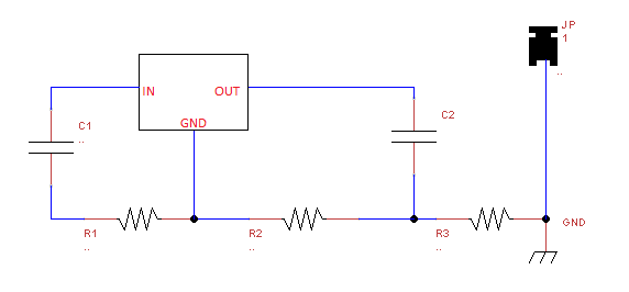
Figure 5: Daisy chain arrangement
Daisy chain arrangement
The above figure showcase the Daisy chain arrangement, notice that all the components are in series, the resistance or impedance of those trace elements sums up, which means that improper grounding arrangements can cause to have different ground voltage. Due to this, the electronic components may get damaged, and the circuit functionality will be compromised since it has no good references.
Star arrangement
The Star arrangement is better compared to the daisy chain due to no summation of resistance and creates a low resistance path to the ground.
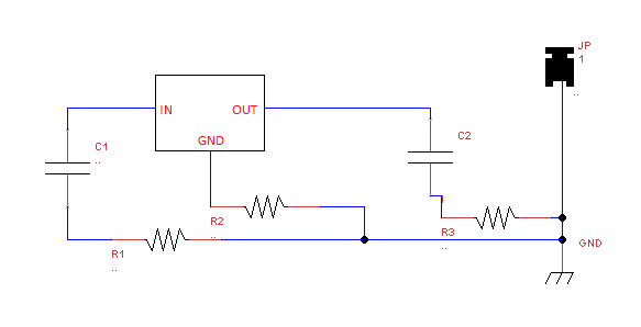
Figure 6: Star arrangement
When the power source is on, the current would flow through the trace, resistor, and then to the ground. The current has to return to the source to make a complete circuit, but in high-speed PCB circuits, the flow of current is not a straight line.
The circuit is similar, but the flow of current will take a longer route across the PCB board. The Parasitic inductance in the board can make the board act like an antenna, which causes EMI related issues.
Connecting ground planes and particularly avoiding ground loop is another crucial factor. Suppose we have a ground plane for a digital part, and the ground plane for the analog power there can be a common ground. But this would be a bad idea, which could cause a potential difference.
Digital circuits must be separated from analog circuits, since digital circuits may induce noise and affect the operation of RF circuits.
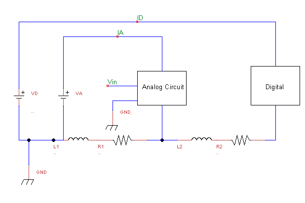
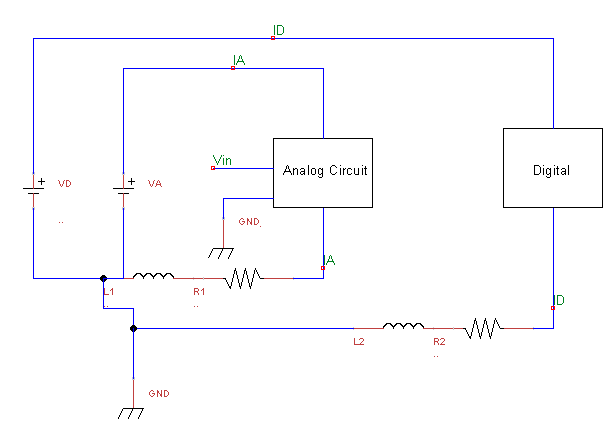
Figure 7 & 8: Importance of ground plane and potential difference
Importance of Kelvin connection
The designer must also emphasize the importance of low-side current-sensing design, achieved through a Kelvin connection.
In the circuit below, if we have to measure the resistance, the most common method would be R=V/I.
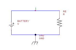
Figure 9: Kelvin Connection
But we tend to ignore the resistance of the wire, since we consider it as very small and negligible, but this creates a stray resistance which causes gain error in the High-speed PCB design. To overcome this we measure the voltage across the resistance.
R=Vr/I
Thus to get optimum performance from an RF circuit board, design engineers must follow the design guidelines recommended by the Manufacturers.
Reference:High Speed Layout Guidelines
1 thought on “Factors affecting High-Speed RF Circuit Design”