It’s a weekend, and it’s time to go down to the pub and put some random steps on the dance floor to your favorite songs of DJ Snake-Lean on, Magenta Riddim. But have you ever wondered how the DJ controls the music and sound equipment at the night clubs?
Ever thought about how the volume of the sound system controlled?

Then we must thank design engineers for inventing the differential amplifiers, which is the basic building block used in volume control circuits and automatic gain control circuits. Let us understand the working of a differential amplifier through circuit simulation using LTSpice tools.
Differential amplifier is the fundamental building block in the CMOS analog integrated circuit design.
There are three different types of differential amplifier
1) Source coupled pair
2) Source cross-coupled pair
3) Current differential amplifier
The diff-amplifier amplifies the difference between the two input signal applied across the input terminal. The output of the differential amplifier is directly proportional to the difference between the two input signals.
The difference between the input signals of the differential amplifier is known as the differential signals. Thus the output of the difference amplifier will be non-zero only if the differential input signal is non zero.
The differential gain of an amplifier calculation shown below.
VO=Ad (V1-V2)
Vd= (V1-V2)
VO=AdVd
Ad=Vo/Vd
If the applied input voltage is differential or they are out of phase with each other. V1 is a sinusoid signal biased at 2.5V with an amplitude of 5mv.
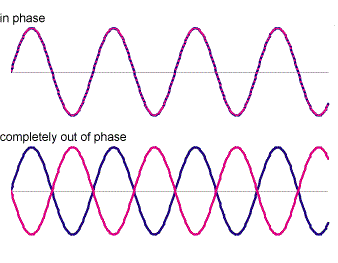
Picture Credit: MCAT Review
In case of a fully differential signal at V2 will be 180 degrees out of phase with V1 biased at 2.5V.
The common-mode voltage
VC=V1+V2/2=2.5
V1=2.5+ 0.05 Sin (wot)
V2=2.5- 0.05 Sin (wot)
For a differential mode voltage, we must subtract the input signal.
VD= (V1-V2)/2
The differential mode voltage will be half of the difference between the two voltages.
VD=0.05Sin (wot)
For an ideal differential amplifier, the differential gain must be infinite and, the common-mode gain to be zero, but in reality, this is not possible.
Differential Amplifier Circuit Generator using LTspice
Let’s start the circuit simulation using LTSpice, to open a new schematic editor. Go to File, click on new schematic. Components required to design a Differential Amplifier are NMOS, PMOS, voltage source, wire, and ground. Now place the NMOS and PMOS in the schematic, click on to the component symbol, and select component symbol popup from the list select the PMOS and NMOS.
Now to mirror the PMOS device, Select M2 and use CTRL+E
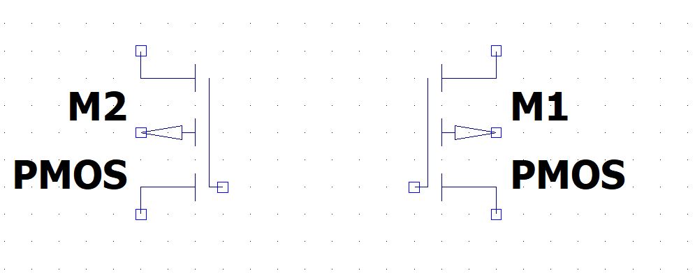
Figure 1: Mirror Function
In this tutorial, we are using the BSIM model to predict the behavior of Differential Amplifier, include the BSIM model text file. For the latest BSIM model, you can download the following model from the link below. In this example we will use Long Channel model.
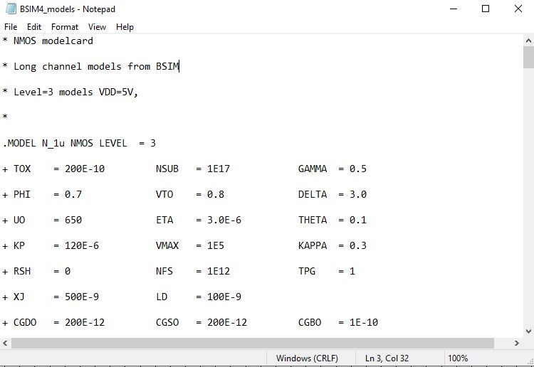
Figure 2 : BSIM4 Model
https://bsim.berkeley.edu/models/bsim4/
Place the PMOS and NMOS on to the schematic, the MOSFET terminal source connected to the bulk or you can use 4 terminal NMOS and PMOS device, which uses the symbol indicates substrate is p-type to n channel. Right-click on the MOSFET and set the size of PMOS and NMOS as shown in the image below. Name the model as P_1u and N_1u as per the BSIM model file included in our simulation.
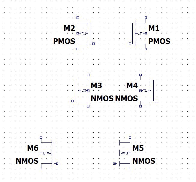
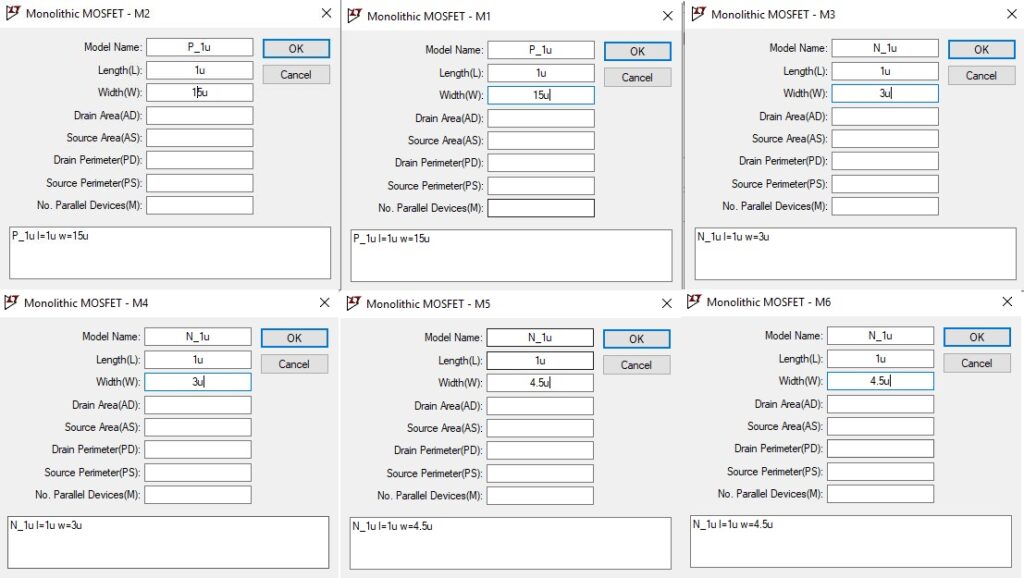
Figure 2: Setting size of the Device
To include the BSIM model file, Go to edit and select SPICE Directive’S’ and then type .include BSIM4_model.txt.
In this tutorial, we must define the VDD, Vbias, V1, V2, IDC, and Vss as an input pin, as shown in fig below. Define the port type as an input or output.
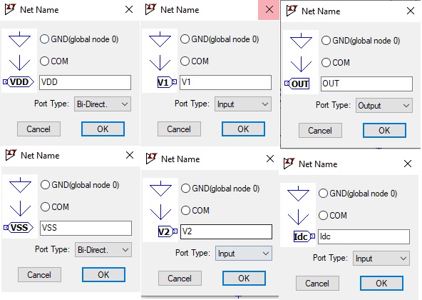
Figure 3: Define Pins
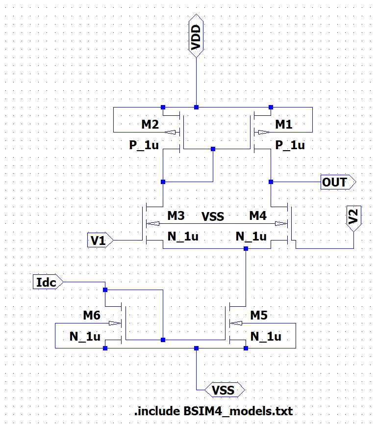
Connect all the pins and the MOSFET shown in the figure below.
Defining the Pins for differential amplifier
Figure 4 : Schematic of Differential Amplifier
Next we will convert this circuit into a symbol.
How to create a symbol in LTSpice?
The next section will guide you on how to create a symbol in LTSpice. Click on Hierarchy and then select create a new symbol you will get a new schematic. Save the symbol as Diff_Amp, this symbol will correspond to the schematic which we had done earlier. Now click on the draw and then click on Line. We will draw the differential amplifier symbol and add the input and output pin to our symbol. Click on the edit and select add pin/port. Name the pins as V1, V2, IDC, VDD, VSS and Vbias for input terminal and OUT the output terminal.
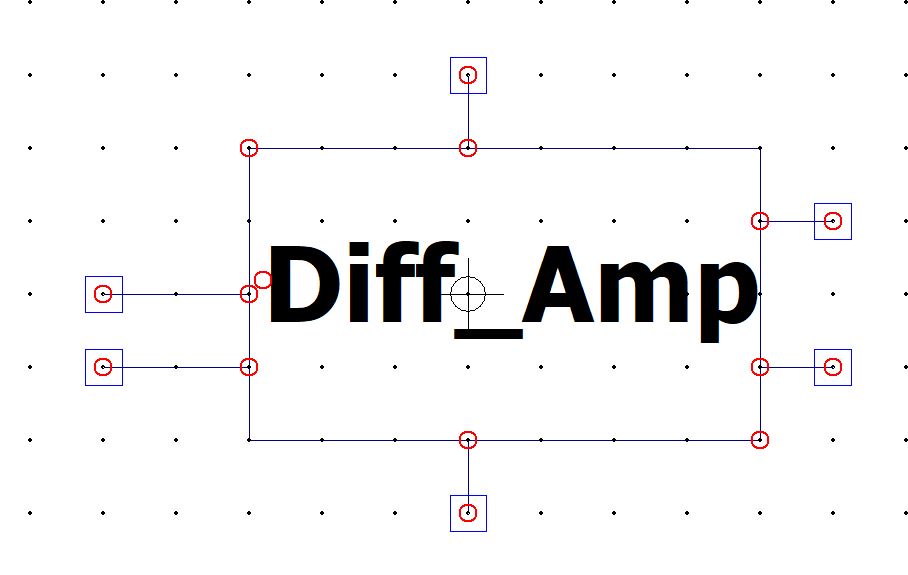
Figure 5: Symbol of Differential amplifier
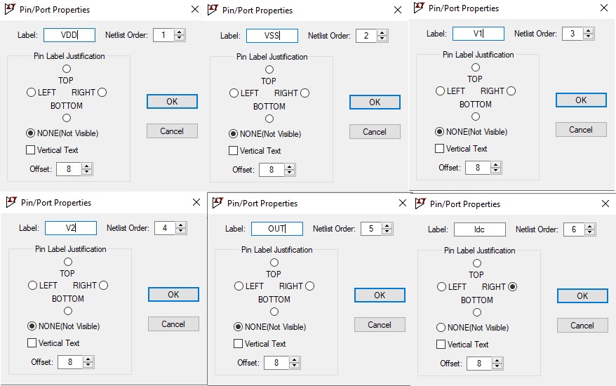
Figure 6: Defining Pins for Symbol
Next, we simulate the circuit for the DC sweep. Open a new schematic. Use the symbol which we had created previously by selecting the component. We must have a voltage source for VDD, Vss, V1, V2, IDC, and Vbias.
| Voltage Source | Volts |
| VDD | 5V |
| Vss | 5V |
| V1 | DC offset-0V, Amplitude-5mV, Frequency-1 KHz, AC amplitude-1 |
| Vbias | 2.5V |
| V2 | GND |
| IDC | 30u |
The first source of sweep will be V1, the start value to be -5, and stop value as 5 with 1mv increment.
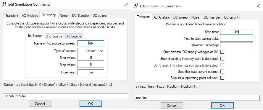
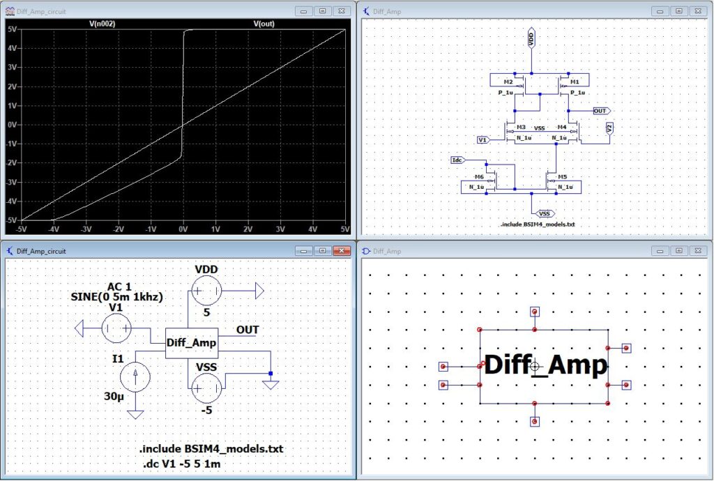
Figure 7: DC analysis of Differential Amplifier
Now let us make a few changes to our voltage source, right-click on voltage, and click on advanced.
Select Sine
Right-click on to the .dc and change from DC sweep to transient analysis.
.tran 4m
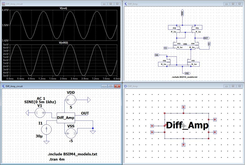
Figure 8: Transient analysis of Differential Amplifier
End of Tutorial.
Hi, how did you work out what sizes you needed the MOSFETs to be to get the gain you want?
Hi Emilia,
It would be based on the transconductance. Since the transconductance and W/L are proportional.
W/L ratio is linked to the transconductance and the current capability, together with the multiplicity factor m. A higher W/L ratio increases the current gain and subsequently a higher current for a given Vg
gm(transconductance)=root(2*uCox*W/L*ID)
assume, uCox = 200uA/V2; ID=1mA
then for gm=2.5mA/V,
W/L= gm2/(2*uCox*ID)=15.625
For more details please check this
https://inst.eecs.berkeley.edu/~ee105/fa98/lectures_fall_98/091898_lecture11.pdf