The Common drain amplifier is a single transistor MOSFET amplifier, one of the basic fundamental MOSFET amplifiers. The Common drain amplifiers are different from Common source amplifiers where the resistor connected across the drain.
Let us analyze the input resistance, output resistance, and the gain of the amplifier. Based on these parameters, it provides insight into how the circuit will interact with other components.
To determine the input resistance, apply the test voltage at input and measure the current flowing out of it.
Voltage source VIN connected to the gate, (gm) (vgs) voltage-dependent current source at the source terminal. When the input voltage is zero, the flow of the current is zero.
Rin= Voltage test/Current test=Infinite
The input resistance is equal to infinity.
To determine the voltage gain of the amplifier, we must determine the output voltage over the input voltage. We represent the Common drain amplifier in the form of a small-signal model.
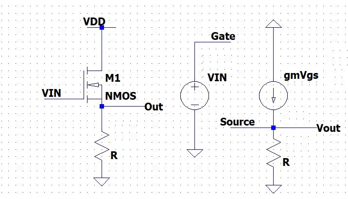
Figure 1: Common Drain Amplifier small signal model
Voltage applied across the gate and source terminals, source of the MOSFET connected to the resistor, and connected to ground. Drain of the MOSFET connected to Vdd, and constant voltage across Vdd of the MOSFET would become small-signal ground. Since the voltage is constant across Vdd, there is no change with respect to the function of time, and consider it as ground.
The voltage drop across the resistor must be equal to the current flowing into it.
Vout= (gm) (vgs) (R)
Vgs=Vg-Vs
Vg is the input voltage applied to the circuit, and Vs is the voltage across the source, the same as the voltage across Vout.
Vout=gm (Vin-Vout) R
Vout/Vin= (gm) (R)/ (1+gmR)
When the value of (gm) (R) approaches infinity, then gain will be positive.
The Common drain amplifier would be a good buffer, which prevents the signal source being affected.
To determine the output resistance of the circuit.
The input voltage applied to the gate terminal, the source terminal connected to the voltage-dependent current source and resistance R. Apply test voltage across source resistor and measure the current across the resistor and short all the independent source.
Test Current= (Test Voltage/ Resistor)-(gm) (vgs)
Vgs=-Vtest
Test Current=-Vtest (1/Resistor + gm)
Rout= (R/ (1+gmR)
Circuit Simulation using LTSpice
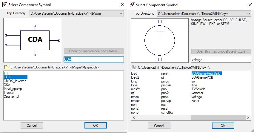
Let’s start the circuit simulation using LTSpice, to open a new schematic editor. Go to File, select the New schematic. Components required to design a Common Drain Amplifier are NMOS, voltage source, wire, and ground. Now place the NMOS in the schematic, click on to the component symbol, and you would get the select component symbol popup from the list select the NMOS.
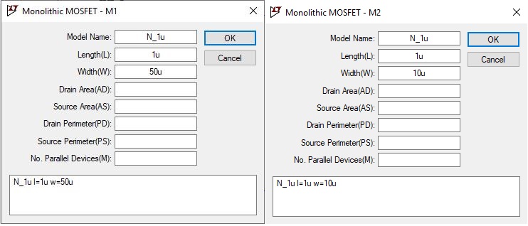
In this tutorial, we are using the BSIM model to predict the behavior of the Common Drain Amplifier, include the BSIM model text file. For the latest BSIM model, you can download the following model from the link below. In this example, we will use the Long Channel model.
https://bsim.berkeley.edu/models/bsim4/
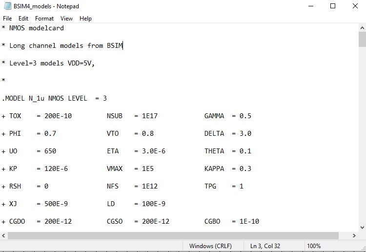
To include the BSIM model file, Go to edit and select SPICE Directive’S’ and then type .include BSIM4_model.txt.
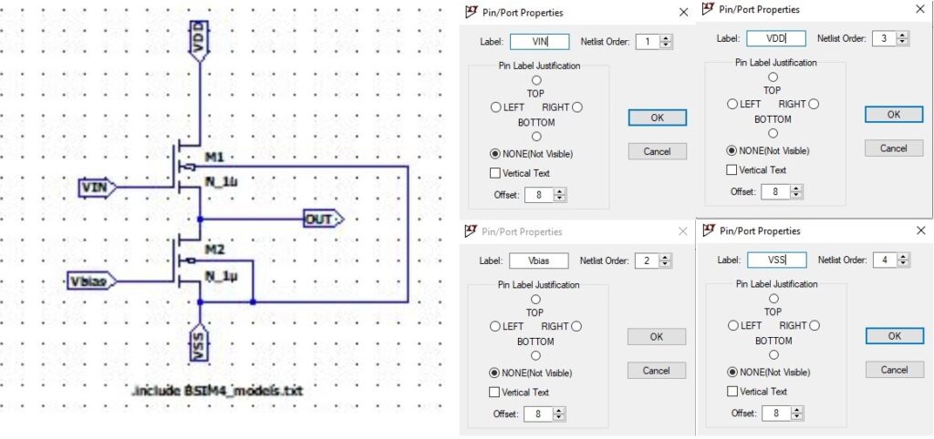
In this tutorial, we must define the VDD, Vbias, VIN, and Vss as an input pin, as shown in fig below. Define the port type as an input or output.
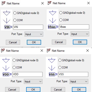
Figure 2: Common Drain Amplifier-Define Pins
Draw the Common Drain Amplifier schematic as shown in figure below, we will convert this circuit into a symbol.
The next section will guide you on how to create a symbol in LTSpice. Click on Hierarchy and then select Create a New Symbol you will get a schematic window. Save the Symbol as CDA, the Symbol will correspond to the schematic which we had done earlier. Now click on the draw and then click on Line. We will draw the CDA symbol and add the input and output pin to our Symbol. Click on the edit and select add pin/port. Name the Pins as VIN, VDD, VSS, and Vbias for input terminal and OUT the output terminal of the Common Drain amplifier.
The Common drain amplifier Symbol is shown in the figure below.
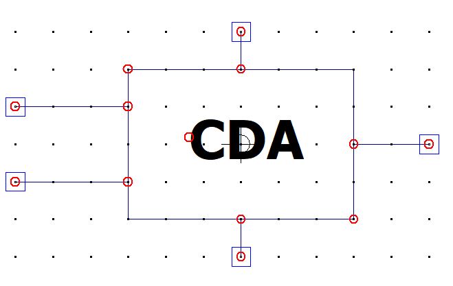
Figure 3: Common Drain Amplifier Symbol
Next, we simulate the Common drain amplifier circuit for the DC sweep. Open a new schematic. Use the Symbol we had created previously by selecting the component. We must have a voltage source for VDD, Vss, VIN, and Vbias.
| Voltage Source | Volts |
| VDD | 5V |
| Vss | -5V |
| Vin | DC offset-0V, Amplitude-5mV, Frequency-1 KHz, AC amplitude-1 |
| Vbias | 2.5V |
The complete Common drain amplifier circuit is shown in figure below.
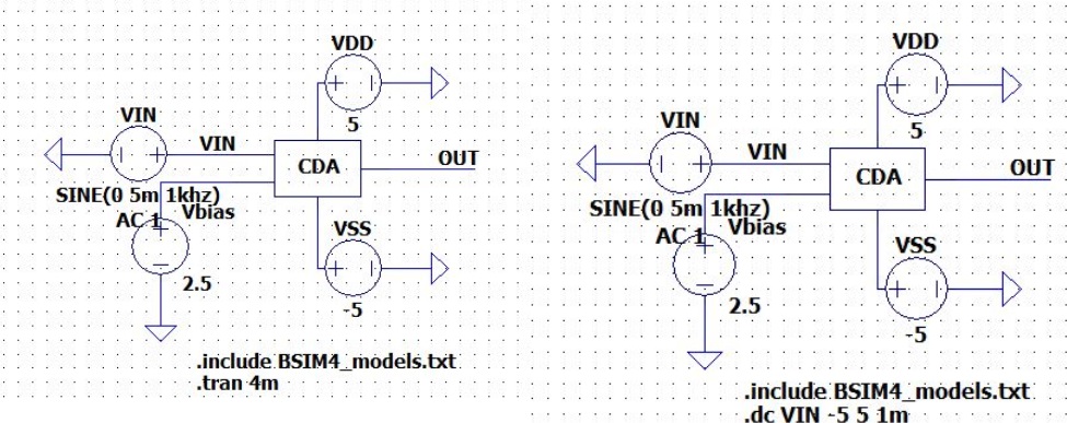
Figure 4: Transient and DC analysis circuit
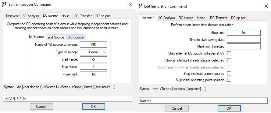
The first source of sweep will be VIN, the start value to be -5, and stop value as 5 with 1mv increment.
Now let us make a few changes to our voltage source, right-click on voltage, and click on advanced.
Select Sine
Right-click on to the .dc and change from DC sweep to transient analysis.
.tran 4m
Run the simulation to plot the DC Sweep and the transient analysis of the Common Drain Amplifier. The simulation results is shown in the figure below
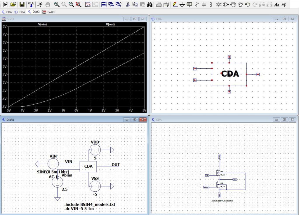
Figure 5: DC analysis
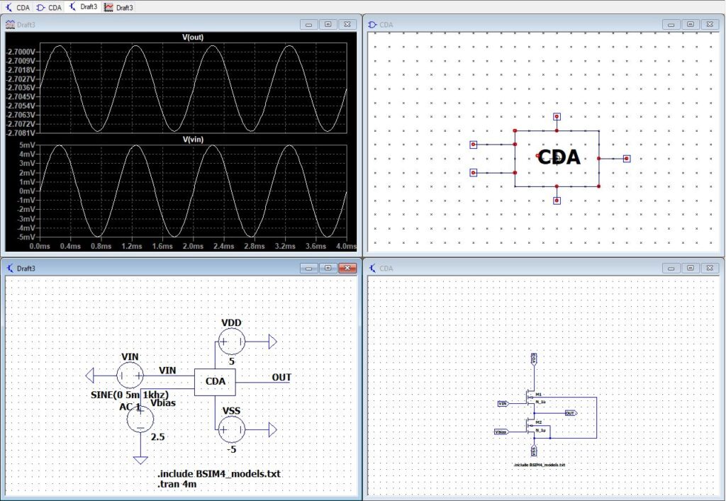
Figure 6: Transient analysis
End of the tutorial.
Great job
It is very instructive and helpful, but could you explain where to find the text file? It isn’t in the downable file.
Hello Juan,
You can download the BSIM4 model file from the link below.
https://drive.google.com/file/d/1uoeCOBqVdoeKjKEmSfaBuxtu3ru3YQrQ/view