In this tutorial, we will simulate the CMOS Inverter using LTSpice XVIII circuit simulation tool. In this CMOS inverter circuit simulation, we will use the BSIM4 Spice model.
What is BSIM4? That might be your next question.
BSIM came into prominence during 1987, known as the Berkeley short-channel IGFET model. Modeling of any device involves the following steps.
1) Processing or fabrication technique.
2) Device simulation, emphasize on device physics.
3) Characterization of the device.
4) Transform into software programming.
BSIM is the first industrial standard MOSFET model, its first CMC standard models in TM12, which enables efficient macro modeling. Professor Don Peterson provided the Spice model free to the industry, which explains the success of the BSIM model. CMOS inverter forms the basic building block of any digital circuit, 90% of integrated circuits fabricated using CMOS technology.
The logical operation of CMOS inverter
| Input | Output |
| 0 | 1 |
| 1 | 0 |
Let’s start the circuit simulation using LTSpice, to open a new schematic editor. Go to File, click on new schematic. Components required to design a CMOS inverter are NMOS, PMOS, voltage source, wire, capacitor, and ground. Now place the NMOS and PMOS in the schematic, click on to the component symbol, and you would get the select component symbol popup from the list select the PMOS and NMOS.
In this tutorial, we are using the BSIM model to predict the behavior of CMOS inverter, include the BSIM model text file. For the latest BSIM model, you can download the following model from the link below.
https://bsim.berkeley.edu/models/bsim4/
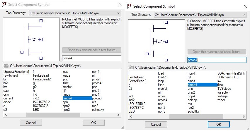
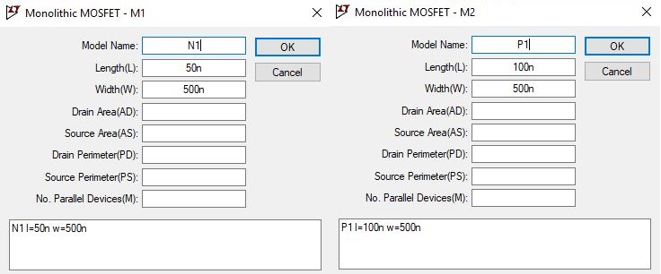
Place the PMOS and NMOS on to the schematic, the MOSFET terminal source connected to the bulk or you can use 4 terminal NMOS and PMOS device, which uses the symbol indicates substrate is p-type to n channel. Right-click on the MOSFET and set the size of PMOS and NMOS and shown in the image below. Name the model as P1 and N1 as per the BSIM model file included in our simulation.
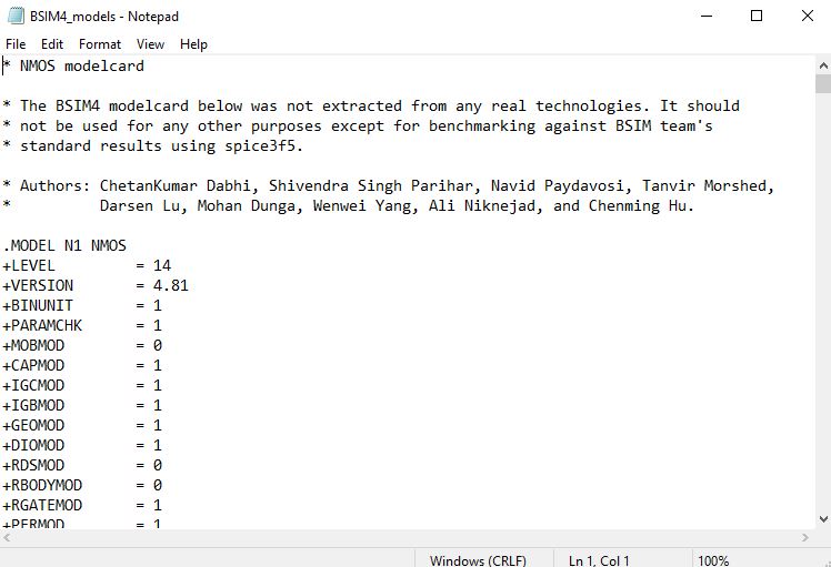
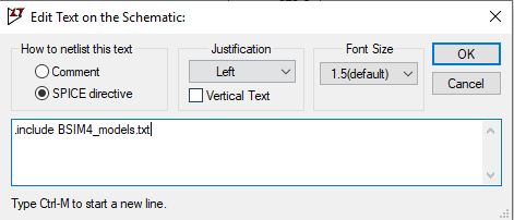
To include the BSIM model file, Go to edit and select SPICE Directive’S’ and then type .include BSIM4_model.txt.
In this tutorial, we must define the VDD and digital ground as an input pin, as shown in fig below. Define the port type as an input or output.
Label the input as IN and output as OUT. When the CMOS inverter input connected to the ground, the output is pulled to VDD through the PMOS device, and when the input is connected to VDD, the output is pulled through the ground by the NMOS device.
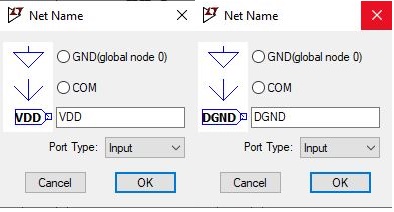
Figure 1: Defining Pins
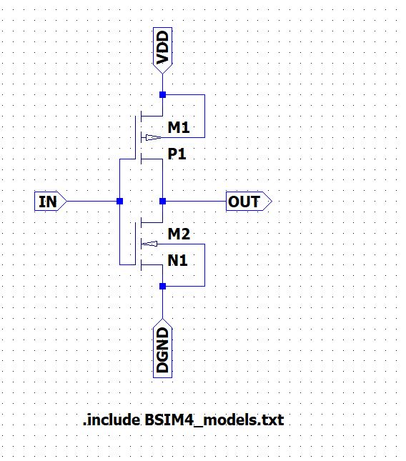
Figure 2: CMOS inverter Schematic
We will convert this circuit into a symbol.
How to create a symbol in LTSpice?
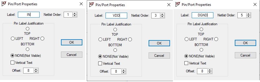
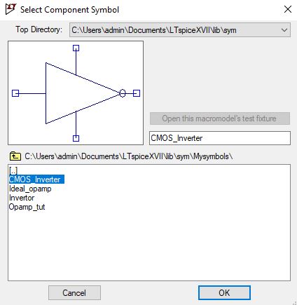
The next section will guide you on how to create a symbol in LTSpice. Click on Hierarchy and then select create a new symbol you will get a new schematic. Save the symbol as CMOS_inverter, this symbol will correspond to the schematic which we had done earlier. Now click on the draw and then click on Line. We will draw the CMOS inverter symbol and add the input and output pin to our symbol. Click on the edit and select add pin/port. Name the pins as IN, VDD, and DGND for input terminal and OUT the output terminal of CMOS Inverter.
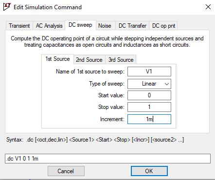
Next, we simulate the CMOS inverter circuit for the DC sweep. Open a new schematic. Use the symbol which we had created previously by selecting the component.

Figure 3: CMOS inverter Symbol generation
Label the VDD input as VDD and output of CMOS inverter as out and define the VDD as the DC source of 1V, as shown in the image below. Connect the ground to the DGND pin and a voltage source to the IN pin of the CMOS inverter.
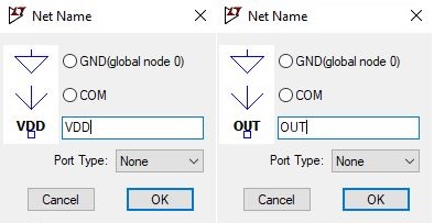
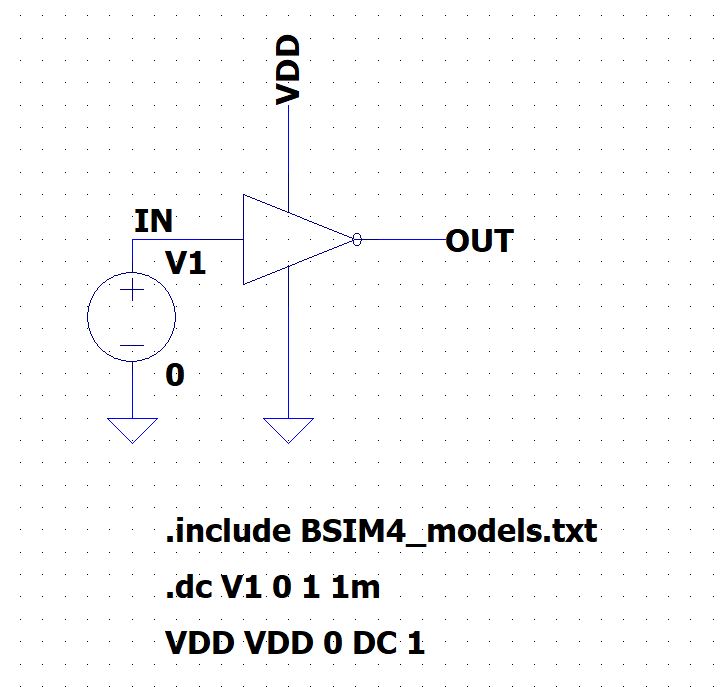
Figure 4: CMOS Inverter DC Sweep Circuit Generator
The first source of sweep will be V1, the start value to be 0, and stop value as 1 with 1mv increment.
Let us place the SPICE analysis on the schematic and run the simulation. Region 1 of the DC characteristics, the input voltage is low, the NMOS is off, and PMOS is ON. As the input voltage increases, both the NMOS and PMOS turn ON. When the input voltage increased further, PMOS turns off, and NMOS fully turns ON.
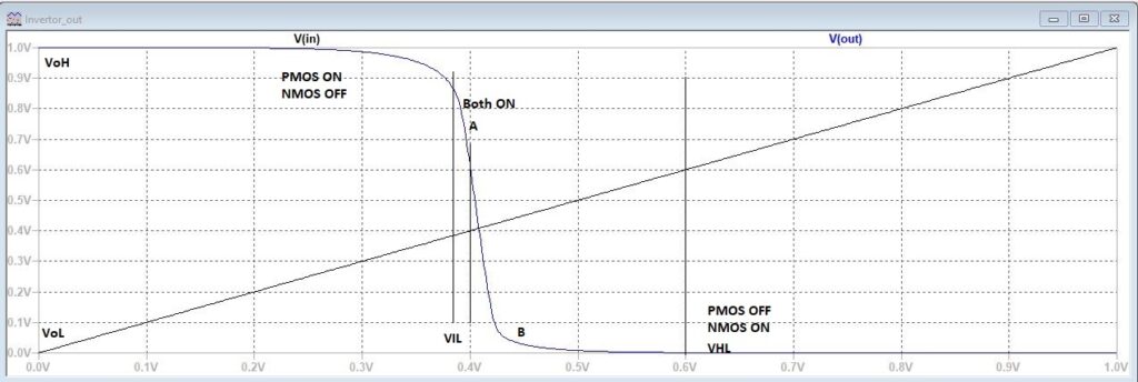
Figure 5: CMOS Inverter DC Sweep analysis
VoH–> Maximum output voltage
VoL–>Minimum output voltage
VIL–>Logic low on the input of inverter
VHL–> Logic high on the input of inverter
Now let us make a few changes to our voltage source, right-click on voltage, and click on advanced.
Select Pulse
Right-click on to the .dc and change from DC sweep to transient analysis.
.tran 2n
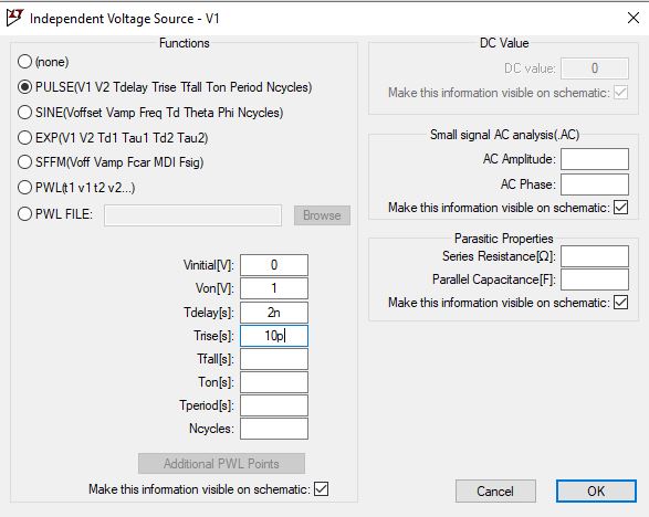
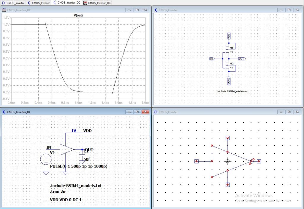
Figure 6: CMOS Inverter transient analysis
End of Tutorial.
2 thoughts on “DC Characteristics of CMOS Inverter using LTSpice circuit simulation”