A design engineer can design an op-amp using the passive components, what is the need of MOSFET based single-stage amplifiers? MOSFET transistors, have an edge over passive components, they can save the chip area. MOSFET, an active device, can produce higher resistance compared to passive load, which would result in higher gains.
Common source amplifier one of the single-stage amplifier with higher gain and output impedance at the cost of lower bandwidth.
Gain of the common source amplifier determined through,
=Resistance in the Drain/Resistance in the Source=Vout/Vin=Av
The Thevenin equivalent of the Common source amplifier with voltage gain Av, shown below.
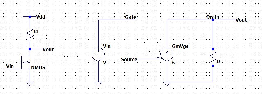
Figure 1: Thevenin equivalent
When we characterize Rin, Rout, and Av, this also means we are characterizing the amplifier.
Voltage source Vin connected to the gate, (gm)(vgs) voltage-dependent current source to the source terminal, and RL to the drain.
Rin=Vin/Iin
When input voltage is applied, what would be the current in the above circuit? There is no place for the current to go, thus the input current is zero. Gain Av, defined as the output voltage/input voltage.
The flow of current in the above circuit is defined as I.
Vout= (0-I) RL=-IRL
Since the initial voltage is zero, this will be equivalent to – (gm) (Vgs) (RL). Vgs will be (Gate voltage- Source Voltage). The gate voltage equal to Vin, the source is grounded, then source voltage is equal to zero.
Vgs=Vin
Vout=-(gm) (RL)
To calculate RL, we consider test voltage applied at the output resulting test current when Vin=0.
RL=Vtest/Itest, when input voltage is equal to zero.
Since Vin is equal to zero, the gate voltage is grounded, and the source is grounded vgs=0. It is an open circuit, and the output resistance will be equal to the load resistance.
Common Source Amplifier Circuit Generator
Let’s start the circuit simulation using LTSpice, to open a new schematic editor. Go to File, click on new schematic. Components required to design a Common Source Amplifier are NMOS, PMOS, voltage source, wire, and ground. Now place the NMOS and PMOS in the schematic, click on to the component symbol, and you would get the select component symbol popup from the list select the PMOS and NMOS.
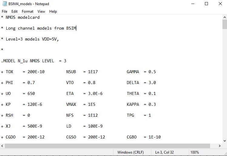
In this tutorial, we are using the BSIM model to predict the behavior of Common Source Amplifier, include the BSIM model text file. For the latest BSIM model, you can download the following model from the link below. In this example we will use Long Channel model.
https://bsim.berkeley.edu/models/bsim4/
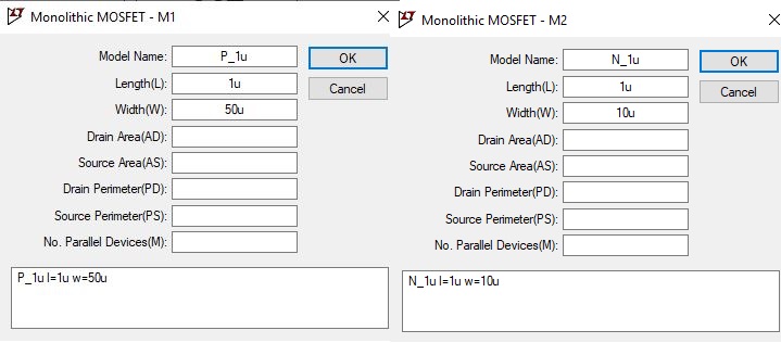
Place the PMOS and NMOS on to the schematic, the MOSFET terminal source connected to the bulk or you can use 4 terminal NMOS and PMOS device, which uses the symbol indicates substrate is p-type to n channel. Right-click on the MOSFET and set the size of PMOS and NMOS and shown in the image below. Name the model as P_1u and N_1u as per the BSIM model file included in our simulation.
To include the BSIM model file, Go to edit and select SPICE Directive’S’ and then type .include BSIM4_model.txt.
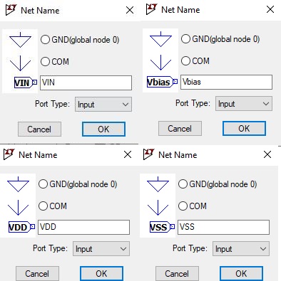
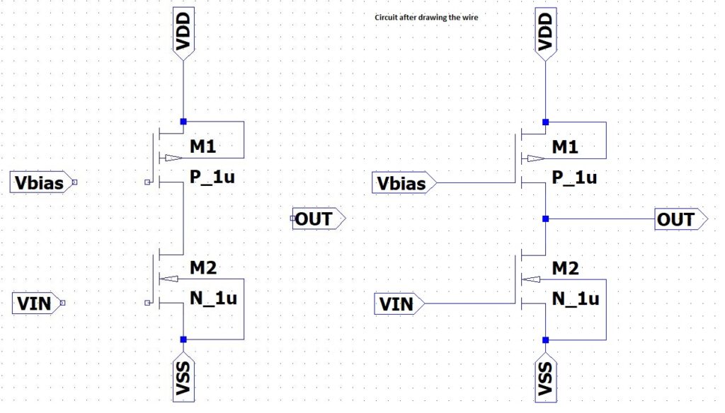
In this tutorial, we must define the VDD, Vbias, VIN, and Vss as an input pin, as shown in fig below. Define the port type as an input or output.
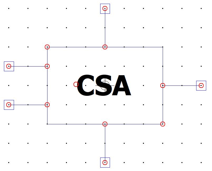
We will convert this circuit into a symbol.
How to create a symbol in LTSpice?
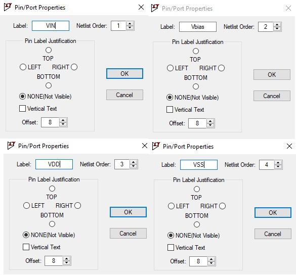
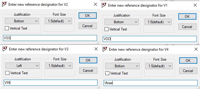
The next section will guide you on how to create a symbol in LTSpice. Click on Hierarchy and then select create a new symbol you will get a new schematic. Save the symbol as CSA, this symbol will correspond to the schematic which we had done earlier. Now click on the draw and then click on Line. We will draw the CSA symbol and add the input and output pin to our symbol. Click on the edit and select add pin/port. Name the pins as VIN, VDD, VSS and Vbias for input terminal and OUT the output terminal of Common source amplifier.
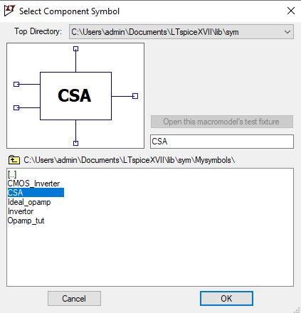
Next, we simulate the Common source amplifier circuit for the DC sweep. Open a new schematic. Use the symbol which we had created previously by selecting the component. We must have a voltage source for VDD, Vss, VIN, and Vbias.
| Voltage Source | Volts |
| VDD | 5V |
| Vss | 5V |
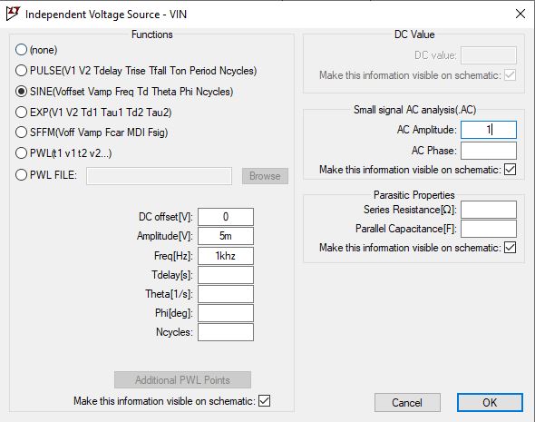
| Vin | DC offset-0V, Amplitude-5mV, Frequency-1 KHz, AC amplitude-1 |
| Vbias | 2.5V |
We will assign the label VSS, VDD, Vin and Vbias in our circuit and the complete Common Source Amplifier circuit is generated.
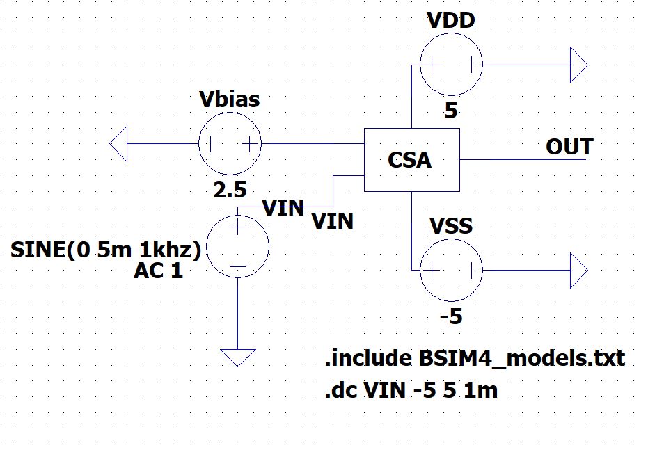
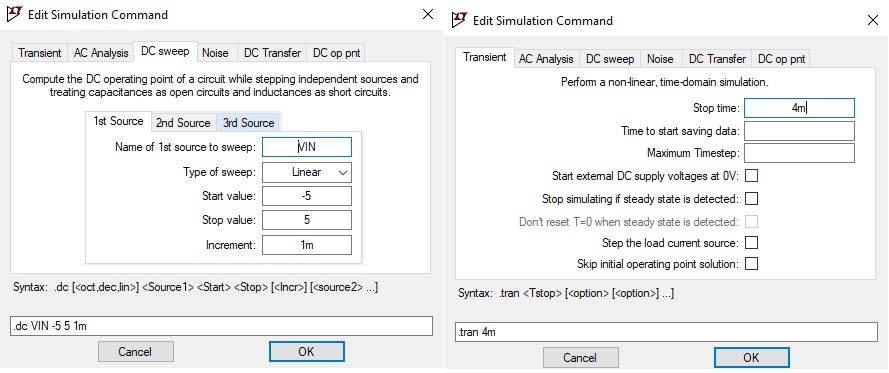
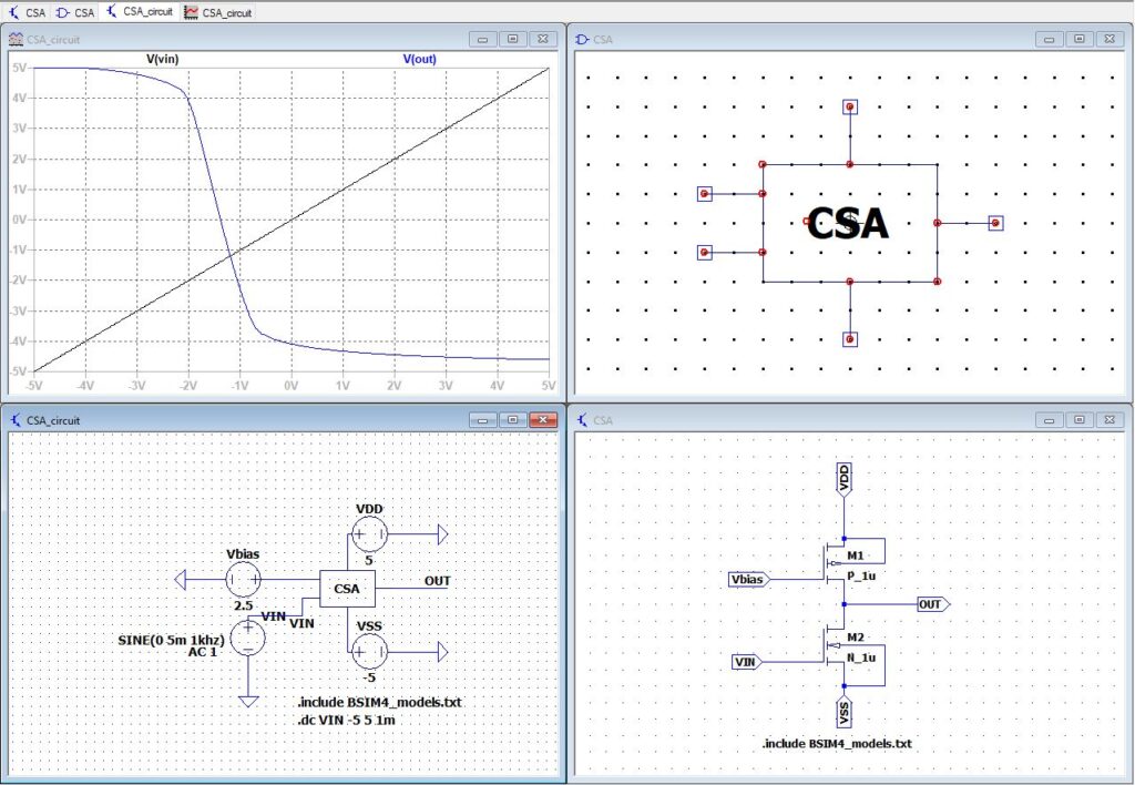
The first source of sweep will be VIN, the start value to be -5, and stop value as 5 with 1mv increment.
Run the simulation, you can check the DC analysis for the Common source amplifier below.
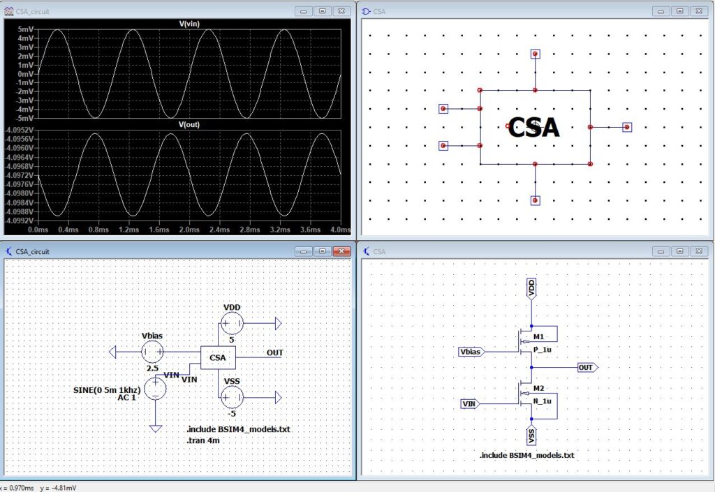
Now let us make a few changes to our voltage source, right-click on voltage, and click on advanced.
Right-click on to the .dc and change from DC sweep to transient analysis.
.tran 4m
Run the simulation, you can check the transient analysis for the Common source amplifier below.
End of tutorial.
1 thought on “Common Source Amplifier Circuit simulation using LTSpice”