Evolution of semiconductor technology
The advancement of semiconductor technology started with vacuum tubes, systems made of these vacuum tubes took entire room space and equivalent to the weight of an elephant.
Remember the Typewriter? Yes, the Typewriter which is almost outdated these days. Even the vacuum tubes, considered to be one of the most important inventions in the semiconductor space, but obsolete due to compact electronic devices such as the transistor, integrated circuits. Computers built during the initial days of 1940, through discrete components that were soldered together had too many complications.
The first electronic general-purpose computer ENIAC consisted of more than 17000 vacuum tubes, 70,000 resistors, 10,000 capacitors, and 7,000 diodes, all of which required 5 million hand-soldered connections. Transistors are much smaller, faster, and more reliable compared to vacuum tubes, but did not solve the tangling wire issue.
The breakthrough in Semiconductor technology by Jack Kilby on inventing integrated circuits considered one of the pioneering developments in the field of semiconductor technology. In 1965 Gordon Moore predicted that approximately every two years, you could fit twice the number of transistors into the same amount of space. Today’s processors, like Snapdragon 845, used in many of the smartphones contain around 5.3 billion transistors. To design such a minute processor, it is not humanly possible, thanks to VLSI software used by design engineers to automatically generate chip design.
Many experts are predicting the end of Moore’s Law, the two critical factors which holdback engineers for further miniaturization.
- Quantum tunneling
- Limitation of Photomask
Day by day, the devices are getting smaller, and we are hitting the threshold, the current materials and technique may not allow us to continue the progress.
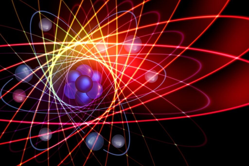
What is quantum mechanics and quantum tunneling?
According to quantum mechanics, the particle is also a wave. A wave also behaves as a particle. A free-electron in a vacuum will be considered a particle. When the force applied towards the free electron, it acquires velocity and momentum.

We can compute the velocity and momentum, as a function of time, by applying Newton’s law. But classical physics doesn’t address how an electron behaves sometimes like particles and sometimes like a wave.
To better understand how the particle also behaves as a wave. We must look into Black body radiation, photoelectric effect, and atomic spectra.
What does the Black body radiation theory state?
When we heat a body to a particular temperature, it will emit radiation. A perfect black body emitter will emit radiation that would have certain traits of wavelength intensity.
When we plot the intensity versus wavelength, we will have the following characteristics, as shown in fig 1 below.
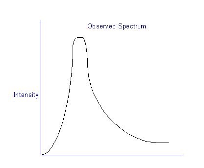
Figure 1: Black body radiation
We can observe that there will be a peak intensity that comes at a specific wavelength about 2900 micrometers divided by the temperature (kelvin). At longer and shorter, wavelengths there will be less radiation. When we compute the spectrum with classical physics, it deviates and not addressable. The intensity that we try to predict goes to infinity as the wavelength gets shorter and shorter.
It was Max Plank in 1901 who discovered a way to explain the characteristics. Max Plank assumed that the energy to be quantized into units of Planks constant
![]()
Next, let us understand the photoelectric effect theory. The light falls over the metal surface, and the number of electrons ejected is measured. Light as a particle has an energy E=hf=hw.
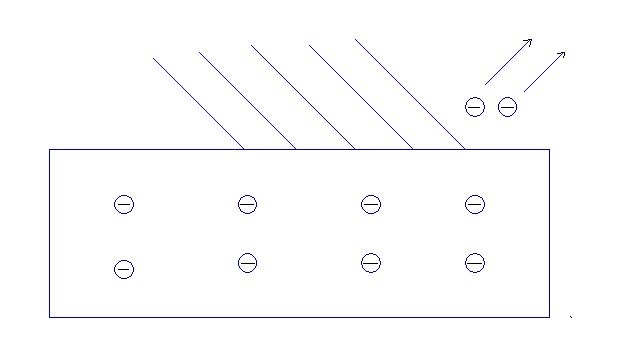
Figure 2 : Photoelectric effect
![]()
When we look into atomic spectra, the light is given off by molecules or atoms. When the atom gets excited, into higher energetic states and once they stabilize, they emit light. The light comes only in the form of discrete colors, not as a continuous spectrum of colors. To measure this discrete energy, we must consider electrons as wave particles.
The frequencies that come off will be the difference between the energy levels, the initial energy minus the final energy divided by planks constant.
Now for our further understanding and discussions, let us consider a particle in a box, and this box goes from 0 to some width L. The potential energy inside the box is 0 but has an infinite barrier in it, and the electron cannot get out of the box.
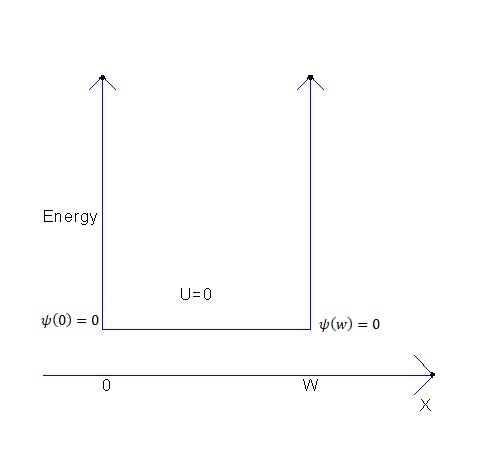
By solving the time-independent equation, and when the boundary conditions are applied. By solving the second-order differential equation, where we first find solutions and then apply the boundary conditions.
![]()
The electron cannot get out of the box, thus no probability to be found at x less than 0 or x greater than W. The appropriate boundary conditions that the wave function has to be 0 at the two ends of the box.
![]()
When an electron confined on the scale of their wavelength, we must consider the quantum effects. To determine the wavelength of the mobile electron in a silicon lattice. We can estimate, with a simple calculation, the relation between momentum and wavenumber.
![]()
𝛌 represent the de-Broglie wavelength of electron.
To determine the wavelength we must find out value p, the average thermal energy of an electron at a given temperature T is 3/2KT.Electron bouncing around in a random thermal motion, in the form of kinetic energy which is determined by P2/2m. Based on the temperature value and the effective mass, we can solve for momentum and then solve for the wavelength.
The wavelength of an electron depends on the effective mass and temperature.
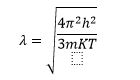
For the silicon material, this would be approximately 10nm at room temperature. The effects of quantum can be observed for 10nm wide quantum well in silicon.
Let us assume that we have a p-type silicon wafer, on top of silicon wafer we have Sio2 which acts as an insulating layer and metal plate on top of Sio2. When a positive voltage is applied to the metal plate, the positive voltage lowers the potential energy of electrons. The positive energy on the plate will attract the negatively charged electrons.
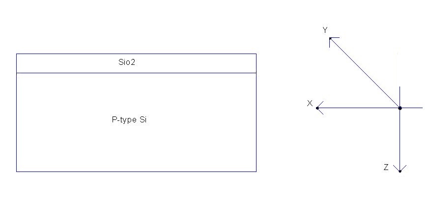
Figure 3: P-type Silicon wafer
Negatively charged electrons will pile up near the interface between the silicon and the insulating layer. The electrons are free to move in the x-y plane but only confined in the Z direction. Thus quantum confinement leads to sub-bands. Now let us consider an electron that encounters a barrier, an energy barrier.
An Electron with energy E encounters a barrier that has higher energy. When we consider classical physics no chance the electron can get over the other side, thus the probability of transmitting across the barrier is 0. According to the quantum mechanics aspect, the electrons are a wave.
If an electron at energy E that is less than the energy of the barrier it encounters then, there is some probability that electron can tunnel or leak through. When an electron that has an energy E, above the top of the barrier, it may not transmit across completely due to reflection.
Process and design engineers must look into the below factors, which is crucial for semiconductor design.
1) Tunneling decreases exponentially with increasing barrier thickness.
2) Tunneling decreases exponentially with an increasing barrier height.
3) Tunneling decreases exponentially with increasing mass.
When we look into the cross-sectional diagram of the MOSFET, the metallic gate electrode where the voltage is applied, underneath the gate, we have a silicon channel. Between the gate and the silicon channel, we have the insulating layer.
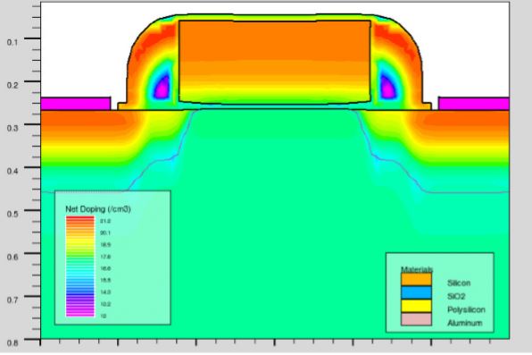
Figure 4: MOSFET Cross Section(Athena Silvaco)
The voltage applied across the gate will influence the potential in silicon. Based on the various technology generations over the past 50 years, for each decade, the gate insulator thinned down and the gate thickness reduced to 1nm, this has led to quantum mechanical tunneling. The current begins to flow from the gate electrode into the silicon this can damage and affect the performance of MOSFET.
Tunneling current due to quantum mechanical tunneling depends exponentially on the thickness of the insulator.Electrons in the semiconductor considered as quantum mechanical particles, thus we cannot consider Newton’s classical law of physics. We need to consider the Schrodinger wave equation, which describes quantum mechanical particles.
What is Quantum computing?
Quantum computing devices work based on the quantum bits or qubits. A qubit can be both 0 and 1 at the same time. There are several physical objects that can be used as Qubit a photon, a nucleus, or an electron.

A qubit can be any two-level quantum systems such as a spin and magnetic field or a single photon. 0 and 1 are the two possible states a classical system can exhibit. But in quantum computers, the qubit doesn’t have to be one of those, since it can be in any proportion of both states at once.
Qubit also exhibits entanglement, each qubit reacts to change in other states instantaneously. When measuring just one entangled qubit, you can directly deduce the properties of other qubits.
An electron can spin up and spin down this correlate to the on and off state of a transistor in a classical computer chip. Quantum entanglement where you can pair multiple particles together so that if you measure the properties of one particle, then automatically know the properties of other particles.
Some of the quantum computer advancements in recent years, by IBM in 2017 announced a 50 qubit chip, Intel announced 48 qubit chip and Google Bristlecone with 72 qubit chip.
Quantum computing will have an impact on the world, which would allow much faster database searches and simulations since the world is growing exponentially. Quantum computing will make a lot of impossible things possible in the future.