Silvaco Altas is a powerful 2D and 3D device simulator that can perform DC, AC, and transient analysis of Silicon, Binary, Ternary, and Quaternary material-based devices.
This tutorial demonstrates the simulation of Silicon MOSFET using Atlas 2D, and we create a Silicon MOSFET structure and perform DC analysis.
The following tool is necessary “S-PISCES” which comes
under ATLAS Module for understanding the device characteristics.
Before working on this example, we must understand the ATLAS input and output information.
Input Information
The input information for ATLAS usually provided in the form of input files. The input file is a text file that can be prepared using DECKBUILD.
The individual lines of the text file are called statements. Each statement consists of a statement name and a set of parameters that specify a certain step of a process simulation or model coefficients used during subsequent simulation steps.
Output information
Run-time output generated by ATLAS will appear in the Deckbuild Text Sub window when running DECKBUILD, or in the current window.
Run time output grouped into two categories.
1) Standard Output.
2) Standard Error Output.
The Standard output consists of output generated from the PRINT.1D Statements or the Extract Statement of Deckbuild.
Standard Error Output consists of the warning & Error messages describing syntax error, file operation errors, system errors.
Order of ATLAS command
1) Structure specification
2) Material & Model specification
3) Numerical Method specification
4) Solution Specification
5) Result Analysis.
Creating an initial Structure
Defining Initial Rectangular grid
Once the Deckbuild is running & the current simulator is set to ATLAS,
Right Click on Commands—->Structure—–>Mesh
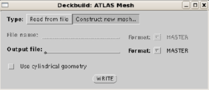
Click on Construct new Mesh
Define the Mesh for the Silicon MOSFET device, with location and spacing.
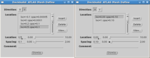
Click on the write button. We get the following statements on the Deckbuild window
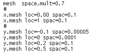
By default the mesh space.mult=1. This value used as a scaling factor for mesh created by X.mesh & Y.mesh statements. A value greater than 1, will create a globally coarser mesh for fast simulation and when a value less than 1, will create a globally finer mesh for the accuracy.
The next step is the initialization substrate for the region. To initialize the substrate structure Right-click on Command—->Structure—->Region
In this Silicon MOSFET Structure, we define three regions.
1) Silicon 2) Silicon oxide 3) Air
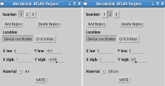
Once we define the device coordinates for all three regions, click on the write button. We get the following statement in Deckbuild.

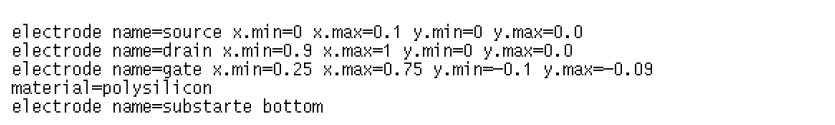
Our next step will be to define the electrodes for the Silicon MOSFET.
Right Click on commands—>Right Click on Structure—>Electrode

In this Device structure, we manually define the electrodes.
In the above input statement, we have defined our desired gate structure through manual editing. After we define all the electrode locations, we click on the write button, and we get the following input statement on the Deckbuild.
Doping of Silicon region
Doping can be done through analytical doping distribution,
General Doping statement
DOPING <Distribution type> <dopant type> <Position Parameter>
Analytical doping profiles can have a uniform, Gaussian, or Complementary error function form. We perform the uniform doping of Silicon material with P-type polarity.
Right Click on Command—>Structure—>Doping—>Analytic

Select the doping profile uniform with polarity Ptype and Conc=1e16, select the region as 3. The direction by default will be set as Y, and click on Write button.
Next, we must perform the Gaussian(with Junction) doping such that we get the NPN Silicon MOSFET structure. Select the doping profile Gaussian(with Junction) with polarity N-type and Conc=1e20, select the region as 3, with 0.15um as junction depth.
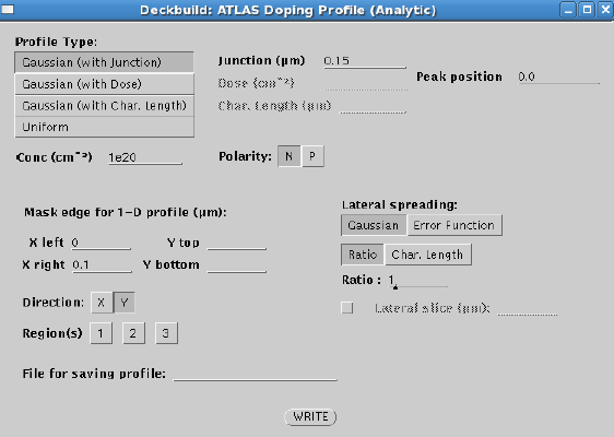
Click on Write button we get the following statement on the Deckbuild

Save the structure file as save outf=air_emb_poly-mos.str
Plot the structure using following input statement in Deckbuild window.
Tonyplot air_emb_poly-mos.str

We need to simulate our electrical characteristics of the MOSFET Device Structure. To obtain the electrical & thermal behavior, Atlas consists of Physical models, specified by using the MODELS & IMPACT statements. The physical models grouped into 5 classes: Mobility, Recombination, Carrier statistics, Implant ionization & tunneling.
Atlas also provides an easy method for selecting the correct models for various technologies. The MOS, BIP, PROGRAM, ERASE parameters for the MODELS statement, which configure a basic set of mobility, recombination, carrier statics & tunneling models.
The MOS & BIP parameter enables the models for MOSFET & bipolar devices, while PROGRAM & ERASE enables the models for programming & erasing programmable devices.
Start the ATLAS simulator with the following command
go atlas
To simulate our electrical characteristics of MOSFET device structure
We need to call our structure file which we had previously saved as
save outf=air_emb_poly_mos.str
Mesh infile=air_mos_poly_mos.str
Specifying Contact Characteristics
An electrode in contact with semiconductor material assumed to be ohmic. We must define the work function so that the electrode treated as a Schottky contact.
CONTACT statement used to specify the metal work function of one or more electrodes.
WORKFUNCTION parameter sets the work function of the electrode.
Eg CONTACT NAME=gate WORKFUNCTION=4.8 sets the workfunction of electrode named gate to 4.8ev. WORKFUNCTION of several commonly used material can be specified using the name of material.
we define the workfunction as N.POLYSILICON
CONTACT NAME=gate N.POLY
Next, we have to specify the physical models specified using the MODELS and IMPACT statements.
We have to define the appropriate model for the above MOSFET Device.
Next, we have to specify the physical models specified using the MODELS and IMPACT statements.
We have to define the appropriate model for the above MOSFET Device.
Right Click on Commands–>Right Click on Models–>Models

In defaults select the device as MOS,
By default the following appropriate model will be enabled,
1) CVT
2) SRH
3) FERMIDIRAC
Click on write button the following input statement will appear on the Deckbuild window.

ATLAS also provides an easy method for selecting the correct models for various technologies. The MOS, BIP, PROGRAM, and ERASE parameters for the MODELS statement configure a basic set of mobility, recombination, carrier statistics, and tunneling models.
To define the appropriate model for MOSFET, define the following input statement on the Deckbuild window.
Model MOS Print
Choosing the Numerical Model
Numerical Solution techniques
Numerical methods are given in the METHOD statements of the input file. Different
combinations of models will require ATLAS to solve up to six equations. There are basically three types of solution techniques
1) Decoupled (GUMMEL)
2) Fully coupled (NEWTON)
3) BLOCK.
GUMMEL method will solve for each unknown in turn keeping the other variable constant, repeating the process until a stable solution is achieved. The NEWTON method solves the total system of unknowns together. The BLOCK methods will solve some equations fully coupled while others are decoupled.
The GUMMEL method is useful where system of equations is weakly coupled but has only linear convergence.
The Newton method is useful when the system of equations is strongly coupled and has
quadratic convergence. NEWTON method may spend more time solving for quantities,
which are essentially constant or weakly coupled. NEWTON also requires a more accurate initial guess to the problem to obtain convergence.
BLOCK method can provide for faster simulations times in these cases over NEWTON.
GUMMEL can provide better initial guess to the problems, so it is better to start the solution with a few GUMMEL iterations to generate better guess, then switch to NEWTON to complete the solution.
In this example we go with Newton method, for more accurate initial guess in order to obtain the Convergence.
Method Newton
Obtaining solutions
Atlas can calculate DC, AC small signal and transient solutions. In this case we usually define the voltages on each of the electrodes in the device. Atlas then calculates the current through each electrode. In all simulations, the device starts with zero bias on all electrodes.Solutions are obtained by stepping the biases on electrodes from this initial equilibrium condition.
Right Click on Commands–>Right Click on Solutions–>Click on solve
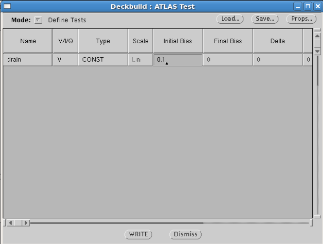
Solve for the Drain voltage.
The voltage on the drain electrode is set to 0.1V and the sequence of solve statement is set to ramp the gate bias. Solution is obtained at 0.25V intervals up to 3.0V.
Solve init
Solve vdrain=0.1
log outf=air_emb_poly_mos.log
Solve vgate=0 vstep=0.1 vfinal=3 name=gate
Tonyplot air_emb_poly_mos.log
We get the characteristic plot for Gate volatge vs Drain Current.

For your reference enclosed the complete statement which you can use on the Deckbuild tool and simulate in Silvaco TCAD tool.
go atlas
#
mesh space.mult=0.7
#
x.mesh loc=0.00 spac=0.1
x.mesh loc=1 spac=0.1
#
y.mesh loc=-0.1 spac=0.00005
y.mesh loc=0 spac=0.0001
y.mesh loc=0.2 spac=0.1
y.mesh loc=0.5 spac=0.1
#
region number=1 x.min=0 x.max=1 y.min=-0.1 y.max=-0.09 material=air
region number=2 x.min=0 x.max=1 y.min=-0.09 y.max=0 material=SiO2
region number=3 x.min=0 x.max=1 y.min=0 y.max=0.5 material=Silicon
#
electrode name=source x.min=0 x.max=0.1 y.min=0 y.max=0.0 electrode name=drain
x.min=0.9 x.max=1 y.min=0 y.max=0.0 electrode name=gate x.min=0.25 x.max=0.75
y.min=-0.1 y.max=-0.09 material=polysilicon electrode name=substarte bottom #
doping uniform conc=1e16 p.type region=3 doping uniform conc=1e18 n.type
x.min=0.25 x.max=0.75 y.min=-0.1 y.max=-0.09 #
doping gaussian junction=0.15 conc=1e19 n.type x.left=0 x.right=0.1 \
y.top=0 y.bottom=0 ratio.lateral=1 #
doping gaussian junction=0.15 conc=1e19 n.type x.left=0.9 x.right=1 \
y.top=0 y.bottom=0 ratio.lateral=1
save outf=air_emb_poly_mos.str
tonyplot air_emb_poly_mos.str
##
go atlas
mesh infile=air_emb_poly_mos.str
contact name=gate n.poly
#
model mos
#
#
method newton itlimit=25 trap atrap=0.5 maxtrap=5 autonr nrcriterion=0.1 \
tol.time=0.005 dt.min=1e-25
solve init
solve vdrain=0.1
log outf=air_emb_poly_mos.log
solve vgate=0 vstep=0.1 vfinal=3 name=gate
extract name=”vt” (xintercept(maxslope(curve(abs(v.”gate”),abs(i.”drain”)))) \
– abs(ave(v.”drain”))/2.0)
tonyplot air_emb_poly_mos.log
2 thoughts on “Tutorial on MOSFET Simulation using Silvaco Atlas tool”