Power consumption is a crucial factor in any VLSI design. The device and gate length has shrunk to nanometers due to increasing transistor counts and speed of operation. Thus low power design techniques becomes a crucial factor.
The modern world surrounded by sophisticated gadgets and, without these gadgets performing day to day tasks is unimaginable. At least once in our lifetime, our smartphone battery would have exhausted and, we have no time to recharge that battery.
When we look into the packaging and cooling cost, this is dependent on the power dissipation of the chip, if engineers cannot reduce the power dissipation, the packaging and cooling cost keeps on increasing. Thus low power circuit design helps to reduce the cost of packaging and cooling.
Modern-day devices have billions of transistors on a single chip, the dimension of the device is getting smaller and smaller due to this it would be challenging to cool down the chip. For any portable device, the battery backup is a crucial factor for the success of any commercial product.
But the battery technology has not matched with the energy requirement consumption. The below diagram depicts the gap between the power consumption and the battery technology energy gap.
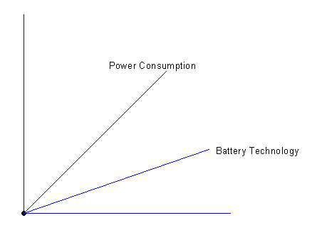
Figure1: Gap between the power consumption and the battery technology energy gap
Another crucial factor for a VLSI chip design is the reliability, as the power consumption increases the temperature also rises, and heat sink design affects the reliability of the chips. For every 10 degree rise in temperature, the failure rate of the chip doubles. Low power chip design will help in improving the reliability of the chip.
How power dissipation affects the functioning of the chip?
Power dissipation is a predominant aspect of VLSI chip design to understand the peak power dissipation refer to the graph below.Power dissipation varies over time, and at some point of time, the dissipation is very high known as peak power or the maximum instantaneous power.
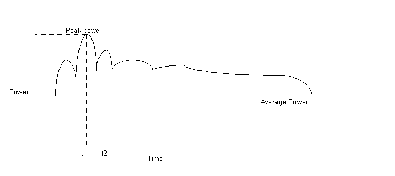
Figure 2: Peak power dissipation graph
The maximum instantaneous power affects the reliability of the system, since the heavy current is drawn and flows through the power line and to the VLSI circuit.Due to the finite resistance in the power line, there will be a voltage drop and causes the glitch and malfunctioning of the chip. Average power affects the packaging and cooling system.
Power is defined as the rate at which energy is drawn from the system or the battery.
Power dissipation with time gives us the energy drawn from the source, which can be in the form of battery for a portable system. Slowing down the clock frequency can reduce dissipation, but this would increase the computation time. In a low power design approach, for a battery-operated system, the energy parameter forms a crucial factor.
Most of the low power circuit design based on CMOS and FINFET technology.
The basic structure of the CMOS circuit consists of a pull-up network and a pulldown network. One of the paramount, disadvantages of the CMOS circuit is the power dissipation due to the glitch and short circuit power dissipation. The source of power dissipation for a typical three input Nand gate using CMOS technology in the figure below.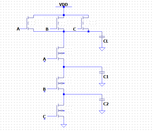
Figure 3: Three input Nand Gate using MOS transistor
Note from the above circuit there are a large number of parasitic capacitances present that causes power dissipation.
Power dissipation in CMOS circuit classified into two types
1) Dynamic Power – When the circuit is in active condition.
2) Static Power- When the circuit is in standby mode.
Power dissipation in standby mode is due to the leakage currents.
Dynamic power dissipation is classified into three type switching power, Short circuit power and, glitching power.
The switching power the most predominant components of power dissipation in CMOS technology. This occurs due to the charging and discharging of the current due to the associated parasitic capacitance. When the output of CMOS is high, the load capacitor Cl will charge from the source through the pull-up network. Then the power dissipated through the pull-up network due to its known resistance.
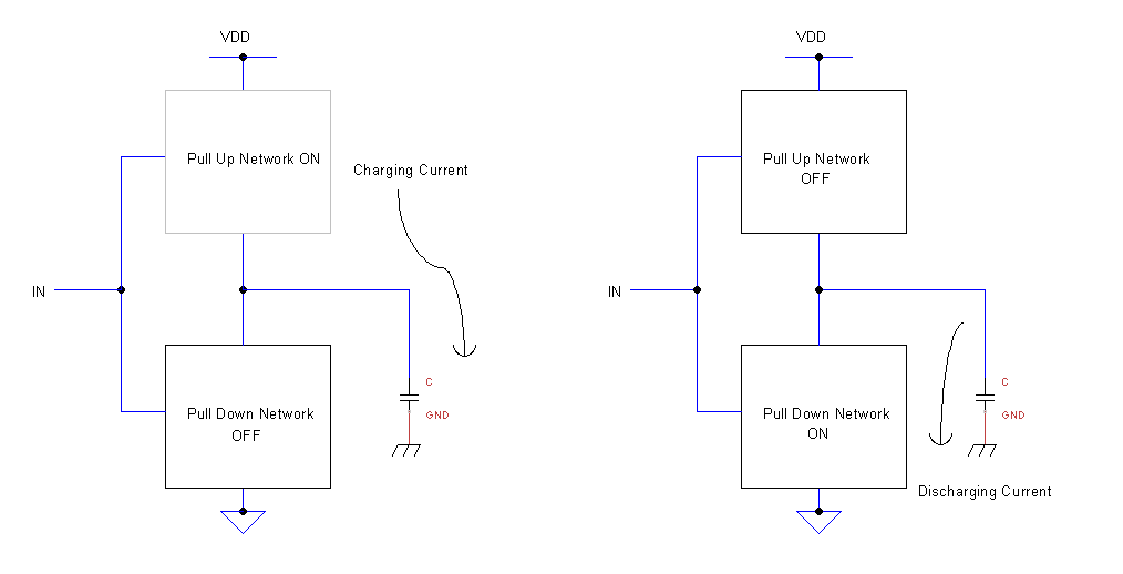
Figure4: Switching power dissipation
When the output is 0, the charge accumulated in the capacitor will discharge through the pull-down network due to finite resistance. Thus switching power dissipation is due to the charging and discharging of parasitic capacitance.
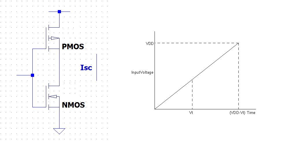
Figure 5: Short circuit power dissipation
Short circuit power dissipation occurs due to a slow change of inputs. As the input voltage increases and reaches the threshold voltage of the pulldown network, the transistor turns on.
As the input voltage increases both, the transistors turn ON and will continue till (VDD-VT). The current inflow will be through the pull-up network to the pulldown network. We define this as short circuit power dissipation, which takes place when there are no load or parasitic capacitors.
What are the different types of leakage current that affects the operation of CMOS transistor?
There are different types of leakage current in CMOS transistor band to band tunneling current, reverse bias p-n junction diode leakage current, subthreshold leakage current, gate oxide tunneling current, gate current due to hot carrier injection, gate induced drain leakage current and channel punch-through current.
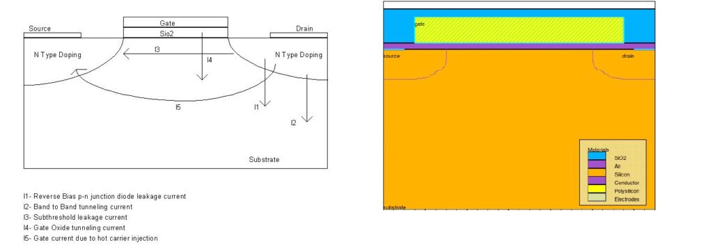
Figure 6: MOS transistor cross-sectional view
MOS transistor cross-sectional view in the above figure, with different types of leakage currents. In the above figure, observe that the transistor with n-type doping with a p-type substrate, which forms a junction. This junction will function as a diode, and this diode will be reverse bias during the normal mode of operation.
Since the diode is in reverse bias, there will be some leakage current. Due to millions of transistors in a chip, the total leakage current can be substantial.
Band to band tunnel current occurs in the junction of transistors, and the electron will go from valence band to conduction band due to the high energy acquired. Whenever the gate voltage is less than the threshold voltage of the transistor, no current flows through the channel. But practically some channel current does flow, and this is the subthreshold leakage current.
CMOS transistor device size is shrinking, and the size of gate oxide is becoming smaller and smaller. Due to the thin silicon dioxide barrier, the electrons cross the silicon dioxide layer leading to the tunneling current.
Since the transistor are getting smaller and smaller, the source and the drain is becoming very close. The current will flow through the channel between source and drain this leakage current is due to channel punch phenomenon.
Recent trends
Taiwan Semiconductor, one of the pioneer semiconductor foundry, has been working on low power technology solutions. TSMC achieved a breakthrough on 22nm ultra-low-power technology, which provides a 10% area reduction and 30% power reduction. Used in applications such as smartphones and fast-moving consumer products. TSMC is investing in R&D activities related to 3 nm and 2 nm CMOS technology, such as 3D transistors and memory devices.
Low power VLSI chip design methodologies are crucial for both system-level and layout levels to increase the efficiency of the chip.