In this Silvaco tutorial, we will design a MOS structure using Athena process simulation tool. Simulate the electrical characteristics using Atlas device simulation tools. We will simulate the transient simulation using an external RC elements.
How to simulate the MOS structure using Athena tools?
For this tutorial, we require Deckbuild interactive tool. Select the Athena process simulation for the simulation of Metal Oxide Semiconductor.
Start the core simulation tool, right-click on Main Control, select the Main Control and set the current simulator as Athena, close the Deckbuild Main Control window.
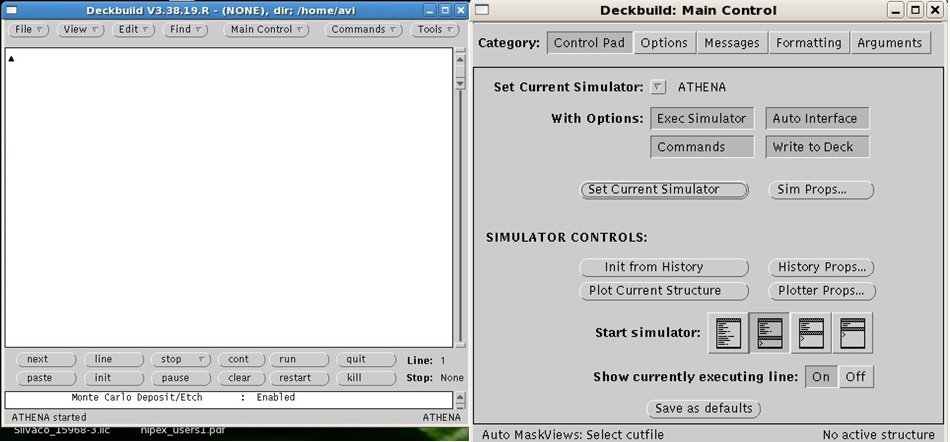
After setting the simulator, the following statement appears on the Deckbuild edit control.
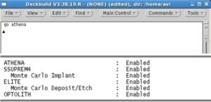
go Athena
All the Process simulation tools under Athena is enabled.
How to create initial structure in Silvaco?
First, define the initial rectangular grid. Right-click on the commands menu, and click mesh-define, and the Athena mesh-define window will pop-up.
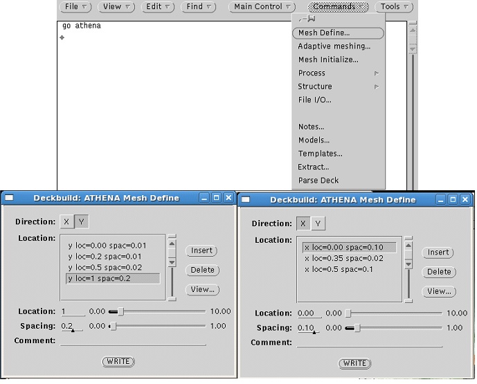
The number of nodes in the grid Np has a direct influence on the simulation accuracy and time. A finer grid should exist in the area where ion implantation will occur due to the junction.
To create the rectangular grid of our specification above.
Click on direction X, click on location, enter the value 0.0, click on spacing, and enter the value 0.10 click on the insert button.
Similarly, enter the other Values of X and the Values of Y as shown above.
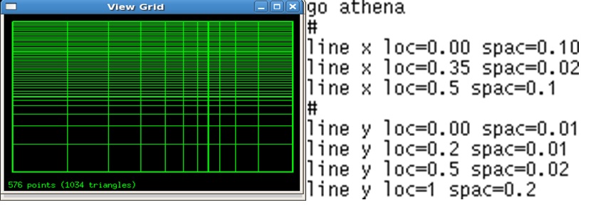
Click on the write button and insert the mesh defined information into the input file. But before doing that, you can have a preview by clicking on the view button. Write the mesh defined information to the file by pressing the write button.
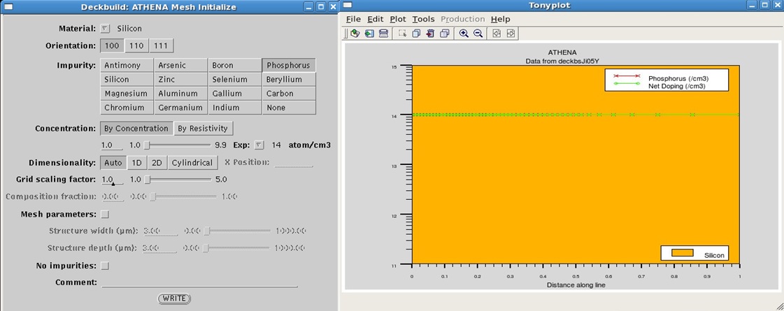
We need to define the initial substrate, select Athena Command menu— >Mesh Initialize.
Mesh Initialize pop-up window appears.
Select the initial material as silicon we define our orientation as [100], the most common one.
In this Silvaco tutorial, the impurity material used phosphorus, and the concentration of impurity as 1e14. When simulating any process involving dopant or diffusion or both, it is critical to use the appropriate model.
The reverse short channel effect in MOS processing is the result of damage-enhanced diffusion.
The level of damage in the semiconductor at any time is not a static quantity but will depend on when & how much damage was induced by a process step & how much annealing has occurred in subsequent thermal steps.
How to select appropriate model in Silvaco tools?
To select the appropriate model, use the METHOD statement. METHOD statement used for two purposes.
The first purpose specifies models for how the damage induced during processes such as implantation or oxidation.
The second purpose is to specify how that damage anneals and diffuses in subsequent or concurrent thermal processes. When impurities are introduced into the silicon lattice, the gradient of the local concentration causes a diffusion process. For a diffusion process, the temperature must be above 800 C for almost all dopants.
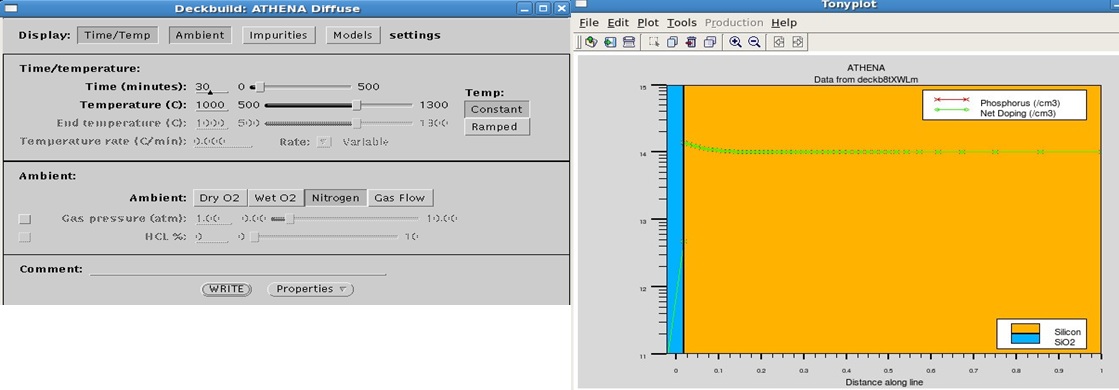
The next step in the process simulation is the formation of the pwell formation through the diffusion process. Open the diffusion menu, right-click on Command—>Process—>Diffuse.
The diffuse menu appears it consist of four sections.
1) Time/Temperature
2) Ambient fields
3) Impurities
4) Models
The minimum set of diffusion step parameters as follows time (60 minutes), temperature (1100 Celsius), Gas pressure (1 atmosphere). After the diffusion process, the formation of a Silicon oxide layer over the silicon surface. Now etch the oxide layer formed during the diffusion process.
Right-click on command—>Process >Etch.
Select the etch method as Geometrical, and select the geometrical type as Dry thickness.
Select the material as oxide that needs to be etched, select thickness to be etched = 0.02um, click on write.
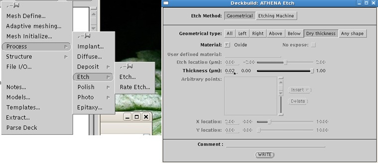
The following statement appears on the Deckbuild input window.
etch oxide dry thick=0.02
An oxide thickness of 0.02 um, etched during the etching process.
How to simulate P-well implant using Silvaco Athena tools?
Ion implantation is a method used to introduce doping impurities into semiconductor device structures. The ion implantation process employs small critical dimensions & shallow doping profiles, high doses.
Right click on Command->Process >Implant.
Implant window will popup.
The following minimum set of parameters should be specified name of implant impurity, implant dose, implant energy, tilt angle in degree.
All other parameters can use their default values. We consider the Dual Pearson model in our simulation example. A beam of fast ions entering crystalline or amorphous solid is slowed down & scattered due to nuclear collision & electronic interaction. The path of Individual moving particles & their collisions modeled utilizing binary collision approximation for a crystalline, polycrystalline, amorphous substance.
After the implantation process, we need to carry out the diffusion process. Select the following parameter for the diffusion process, and click on the write button. The following input statement appears on the deckbuild window.
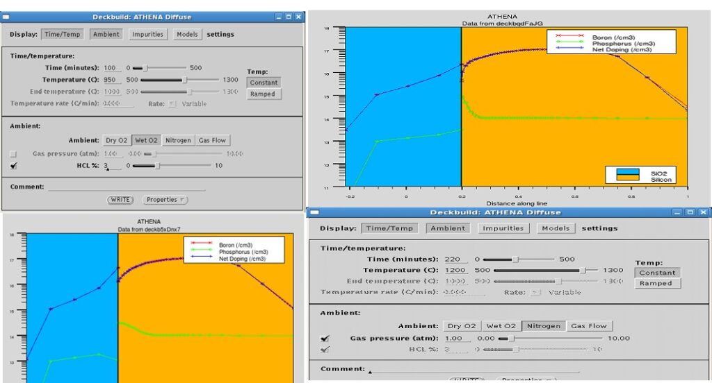
diffus time=100 temp=950 wet02 hcl.pc=3
Click on the write button the following input statement appears on the deckbuild window
diffus time=220 temp=1200 dry02 nitro press=1
Etch the oxide layer over the Silicon surface with the following input statement.
Etch oxide all
To etch the Oxide in the structure, right-click on command->process>etch.
Athena Etch window will appear, select the Geometrical type as all, and select the material as Oxide.
Click on the write button the following statement appears on the deckbuild window.
Etch oxide all
Generate the SiO2 layer for the Sacrificial “Cleaning” oxide and later on etch the SiO2 completely. Follow the similar procedure of diffusion & etch process we had done earlier.
diffus time=20 temp=1000 dryo2 press=1 hcl=3
etch oxide all
The next step in our process simulation is the formation of gate oxide, done through diffusion.
Right Click on Command->Process >Diffuse
diffus time=10 temp=950 dry02 press=1.00 hcl.pc=3
How to extract the thickness of the gate oxide in Silvaco tool?
To extract the thickness of the gateoxide layer formed over the Silicon Layer. Right Click on Command->Extract.
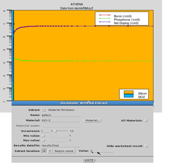
Enter the following parameter click on write.
The following statement appear on Deckbuild window,
extract name=”Gateox” thickness material=”sio2″ mat.occno=1 x.val=0.05
implant bf2 dose=1.2e12 energy=35 crystal
Conformal deposition technique used to generate multi-layered structures.
The conformal deposition technique is used in the oxidation of planar or Quasi planar semiconductor regions.
To set the conformal deposition, right-click on Process—>Deposit >Deposit.
Athena deposit menu will appear.
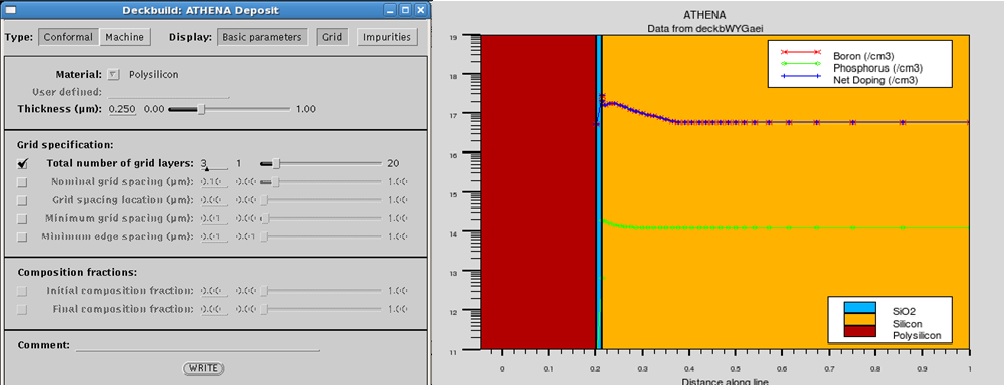
In this Silvaco tutorial, we use polysilicon as our material, with thickness=0.250 and the total number of grid layers as 3.
deposit polysilicon thick=0.250 division=3
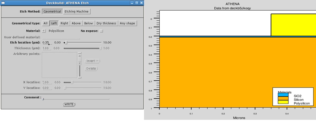
Click on the write button the following statement appears on the deckbuild window.
Etch polysilicon left p1.x=0.35
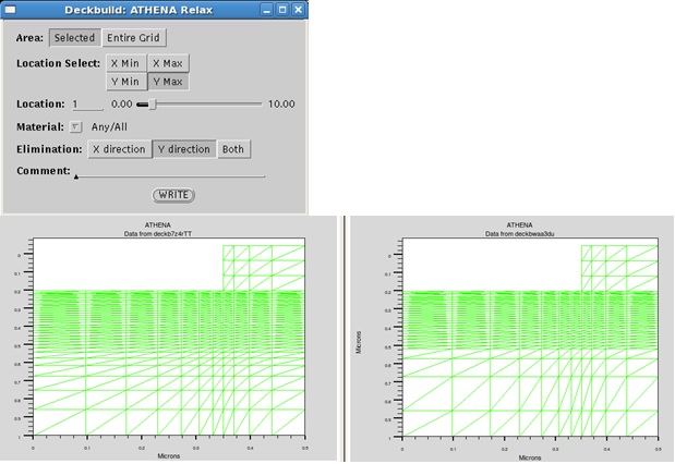
Now let us loosen the grid in Athena Mesh within the user-specified area, so we use the relax statement.
Right-click on Command->Structure->Relax
You can see the relaxation difference between the grid structures. When simulating, an appropriate method statement needs to be selected.
Purpose of method statement
The first purpose determines how damage is induced during the process, such as implantation & oxidation.
The second purpose is to specify how that damage anneals & diffuse in subsequent.
In this Silvaco tutorial, we will use the Method fermi model.
The Fermi Model assumes that point defect populations are in thermodynamical equilibrium and thus need no direct representation. All effects of the point defects on dopant diffusion are built into the pair diffusivity. The Fermi model cannot deal with certain process conditions in which the defect populations are not in equilibrium, such as in wet oxidation.
To select the Fermi model, right-click on the Command menu>Process>Diffuse.
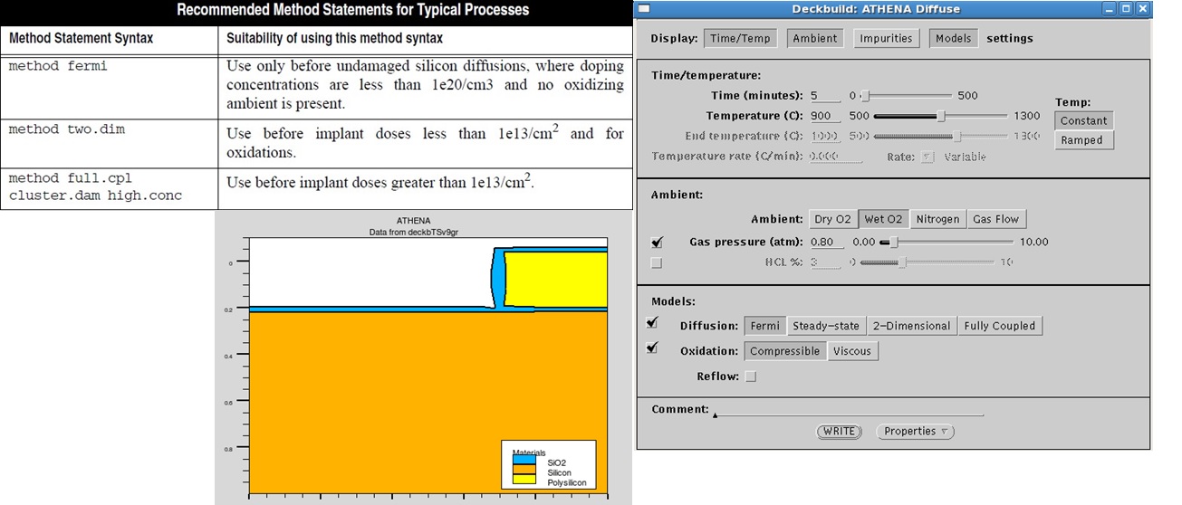
Athena Diffuse window will pop up select models click on diffusion & select fermi.
Click on the write button, and the following input statement appears on the deckbuild window.
method fermi compress
diffus time=5 temp=900 weto2 press=0.8
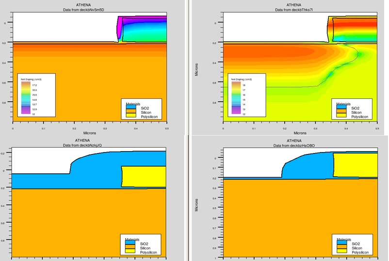
Now we need to introduce phosphorus as our dopant material done through the implant process.
Click on the write button, following statement will be on the deckbuild window.
implant phosphor dose=3e13 energy=50 tilt=0 rotation=0 crystal
In this Silvaco tutorial, to plot the Structure, use the Tonyplot interactive tool. You can see the difference in the net doping and junction formation before after the implantation of phosphorous.
Now let us continue with the sacrificial cleaning oxide process, right-click on Command-> Process>Deposit
deposit oxide thick=0.150 divisions=5
Next, etch the oxide formed by the deposition process.
etch oxide dry thick=0.155
Due to the arsenic implantation, you can see the difference in the net doping of metal oxide semiconductor structure.
Follow the diffusion process by using the fermi compression method.
method fermi compress
diffuse time=5 temp=900 nitro press=1.0
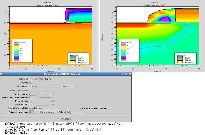
How to extract the Junction depth of the metal oxide semiconductor?
Right click on ->Command>Extract.
Click on the write button.
extract name=”xj” xj material=”silicon” mat.occno=1 x.val=0.1 junc.occno=1
Next, we need to etch the oxide layer from location x=0 to x=0.15, to define the source and drain for the metal oxide semiconductor structure.
Etch oxide left p1.x=0.15
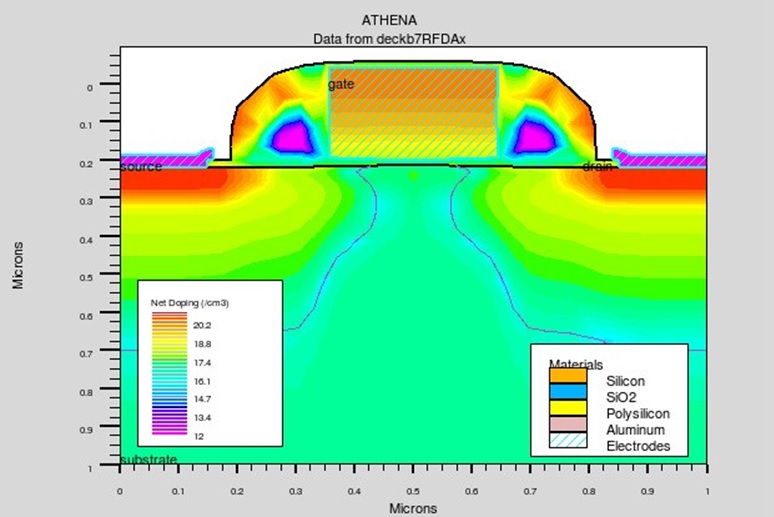
After the etching process, we need to deposit the aluminum metal contact, which will act as a source, and drain for the Metal-oxide semiconductor structure.
Right-click->Command->Process>Deposit.
deposit aluminum thick=0.03 division=2
How to mirror the structure in the Silvaco Athena tool?
To mirror the above MOS structure.
Right Click->Command->Structure->Mirror.
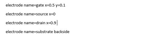
In this Silvaco tutorial, we need to define the electrode for the MOS structure. Right-click->Command->Structure->Electrode. Define the gate, source, drain, and Substrate for the above MOS structure.
Similarly, define the electrode name for gate, source, and drain the following input statement will appear on the Deckbuild window.
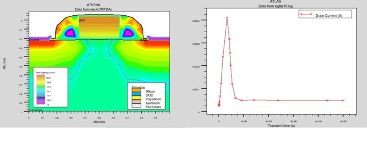
To plot the complete MOS structure, we will use the Tonyplot interactive tool.
Silvaco tutorial on how to simulate the electrical behavior
To obtain these electrical & thermal behavior Atlas consist of physical models specified using the MODELS & IMPACT statements.
The physical models are grouped into five classes: Mobility, Recombination, Carrier Statistics, Implant ionization & tunneling.
Atlas also provides an easy method for selecting the correct models for various technologies. The MOS, BIP, PROGRAM, ERASE statement configure a basic set of mobility, recombination, carrier statics & tunneling models.
The MOS & BIP parameter enables the models for MOSFET & bipolar devices, while PROGRAM & ERASE enables the models for programming & erasing programmable devices.
To change the simulator to Atlas.
Right-click->Main Control->Deckbuild Main Control Window will appear.
Select Atlas as the current simulator.
The following statement will display on the Deckbuild window.
go atlas
The parameter MOS enables Shockley-Read-Hall(SRH), Fermi Statistics(FERMI) & Lombardi Mobility model(CVT). We can input a statement in Deckbuild window that include all the physical mechanism and various parameter.
models mos
For accurate simulation of the MOS devices, the interface charge at oxide, specify semiconductor interface. By setting up the QF parameters for the INTERFACE statement.
Plus, define the work function for the Polygate and interface charge.
Click on the write button.
The following the input statement will appear on Deckbuild.
contact name=gate n.poly
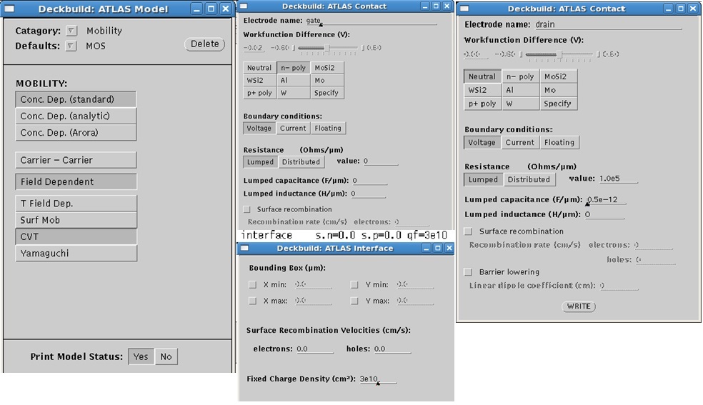
In this Silvaco tutorial, we need to define the external RC Elements to make an NMOS transistor, where we will set the capacitance to 0.5pF/um.
Click on the write button, the input statement will appear on the Deckbuild window.
Contact name=drain neutral resistance=1.0e5 cap=5.0e-13
Silvaco tutorial on choosing the appropriate numerical model
Numerical methods are mentioned in the METHOD statements of the input file. Different combinations of models will require ATLAS to solve up to six equations. There are three types of solution techniques
- Decoupled (GUMMEL)
- Fully coupled (NEWTON)
- BLOCK
GUMMEL method will solve for each unknown in turn keeping the other variable constant, repeating the process until a stable solution achieved.
The NEWTON method solves the total system of unknowns together. The BLOCK methods will solve some equations fully coupled while others are de-coupled.
Right-click->Command->Solutions->Method.
Click on the write button the input statement will appear on the Deckbuild window.
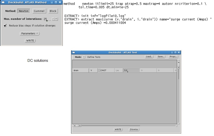
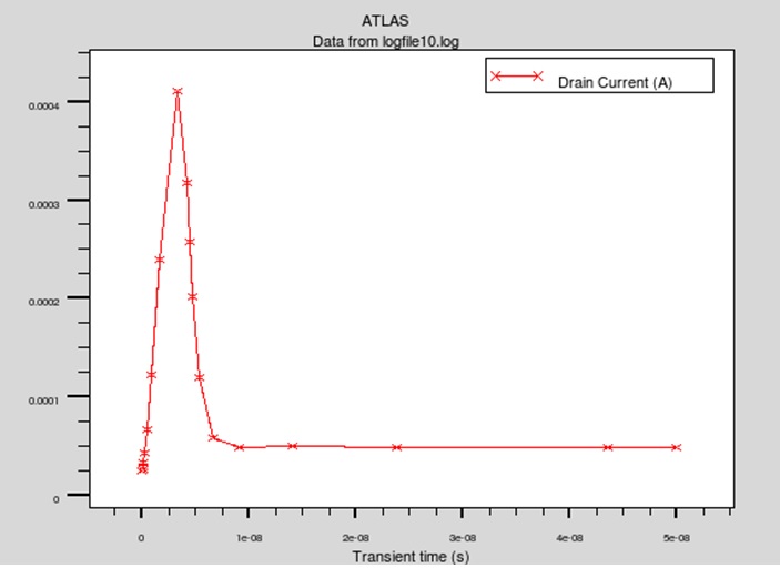
To store the value of the transient results, define the following command on the deckbuild window.
Log outf=logfile10.log
Apply the Gate turn-on transient.
Right-click->Command->Solution->Solve
Enter the value for Gate turn on transient
The following input statement appears on the Deckbuild window.
Solve Vgate=5 ramptime=5e-09 dt=2e-11 tstop=50e-09
Now let us extract the surge current of the MOS structure.
Right-click->command>extract->Device
Select user-defined.
extract max(curve(v.”drain”, i.”drain”)) name=”Surge Current (Amps)
In this Silvaco tutorial, to plot the drain current versus transient time, type the following command on the Deckbuild window.
tonyplot logfile10.log