This tutorial demonstrates how to simulate a diode using Atlas 2D, and we create a silicon diode structure and perform DC analysis.
The following tool is necessary “S-PISCES” which comes under ATLAS Module for understanding the device characteristics.
Before working on this example, let us understand what is a diode?
A diode is a device or a component that allows current to flow in only one direction. The above figure depicts the symbol of a diode, the left side of the diode is the anode, and the right side of the diode is the cathode.
The anode consists of p-type semiconductor material, and the cathode consists of n-type semiconductor material.
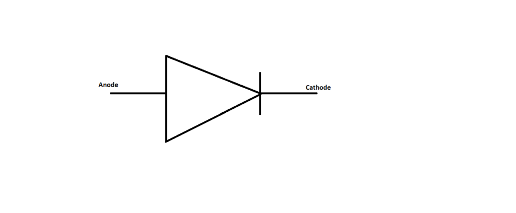
The positive terminal of the battery connected across the anode and the negative terminal connected across the cathode, the diode will conduct when the applied voltage is above 0.7 volts for a silicon-based diodes.
When the positive terminal is on the p-type and negative terminal is on n-type, then the diode is in forward bias mode. When the polarity is reversed the positive terminal is on the n-type, and the negative terminal is on the p-type then the diode is in reverse bias mode.
Input and Output information to simulate a diode
Before working on this example, we must understand the ATLAS input and output information.
Input Information
The input information for ATLAS usually provided in the form of input files. The input file is a text file that can be prepared using DECKBUILD.
The individual lines of the text file are called statements. Each statement consists of a statement name and a set of parameters that specify a certain step of a process simulation or model coefficients used during subsequent simulation steps.
Output information
Run-time output generated by ATLAS will appear in the Deckbuild Text Sub window when running DECKBUILD, or in the current window.
Run time output grouped into two categories.
1) Standard Output.
2) Standard Error Output.
The Standard output consists of output generated from the PRINT.1D Statements or the Extract Statement of Deckbuild.
Standard Error Output consists of the warning & Error messages describing syntax error, file operation errors, system errors.
Order of Atlas command
1) Structure specification
2) Material & Model specification
3) Numerical Method specification
4) Solution Specification
5) Result Analysis.
Let us start working on schottky diode simulation using Atlas tool, ensure that you open a Deckbuild window, and the current simulator in Deckbuild is set to Atlas.
Right click on Main Control. Click on Main Control you will get Deck Build Main Control
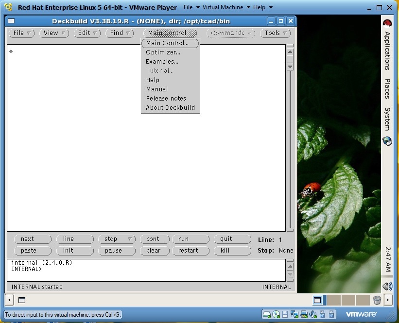
Right Click on Set Current Simulator
Simulator window appears you can select any one of the Simulator (eg Athena, Atlas, Victory).
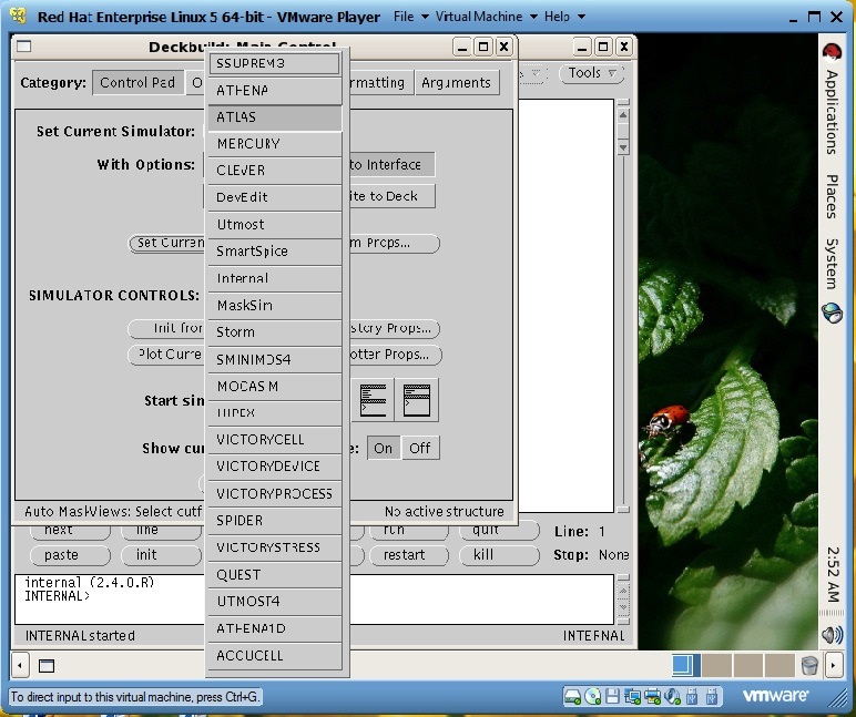
For this example current simulator must be Atlas, we can also run the Atlas simulator by typing “go atlas” command in the Deckbuild Window.
Simulate Diode Forward Characteristics using Silvaco
This tutorial will demonstrate
1) How to generate a device structure using Silvaco Atlas 2D
2) Simulation of Schottky barrier height for anode
3) Forward biasing characteristics of Schottky diode
To design a device structure in Silvaco atlas, we must create an input mesh, define the region and electrodes, and then the doping distribution.
Creating a mesh
Right click on Commands, then right click on Structure then click on Mesh the following window will open which is shown below
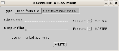
Now we need to construct new mesh so click on Construct new mesh
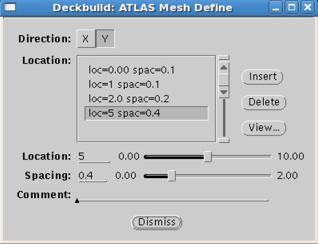
After the inserting following location & spacing click on write.
So you will get the following input file in the Deckbuild window.
go atlas
mesh space.mult=1.0
#
x.mesh loc=0.00 spac=0.5
x.mesh loc=3.00 spac=0.2
x.mesh loc=5.00 spac=0.25
x.mesh loc=7.00 spac=0.25
x.mesh loc=9.00 spac=0.2
x.mesh loc=12.00 spac=0.5
#
y.mesh loc=0.00 spac=0.1
y.mesh loc=1.00 spac=0.1
y.mesh loc=2.00 spac=0.2
y.mesh loc=5.00 spac=0.4
By default the mesh space.mult=1. This value used as a scaling factor for mesh created by X.mesh & Y.mesh statements. A value greater than 1, will create a globally coarser mesh for fast simulation, and when a value less than 1, will create a globally finer mesh for the accuracy.
Defining the regions
Right click on Commands right click on Structure then click on Regions
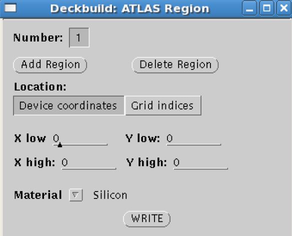
Select Add region the above window will open select material as Silicon click on Write
The following input will be added in Deckbuild.
region number=1 material=silicon.
Once the region is defined, we must define the electrodes for the schottky diode.
Right click on Commands, then Right click on Structure and in the end click on Electrode.
Click on add electrode and select anode & cathode, next we must define location and contact.
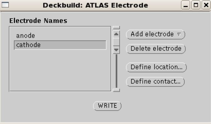
Atlas provides several Boundary conditions.
1) Ohmic contact
2) Schottky Contact
3) Current boundary Conditions.
4) Lumped elements
5) Distributed Contact Resistance.
In this example we need to define the a schottky contact so we must specify the work function(ev) using work function parameter of the Contact statement.
In practice, the workfunction is defined as
WORKFUN= AFFINITY+ΦB
Where ΦB is the barrier height at the metal-semiconductor interface in eV. For example, if the Schottky contact is aluminum with a workfunction difference to the silicon of 4.2eV and a barrier height of 0.7eV, then WORKFUN=4.9.
The Input statement in the Deckbuild window will as given below.

Doping distribution for the Schottky diode
Now we must added the impurities to the semiconductor material for the purpose of modulating its electrical property.
Right Click on Commands…Right Click on Structure….Right Click on Doping….Click on Analytic
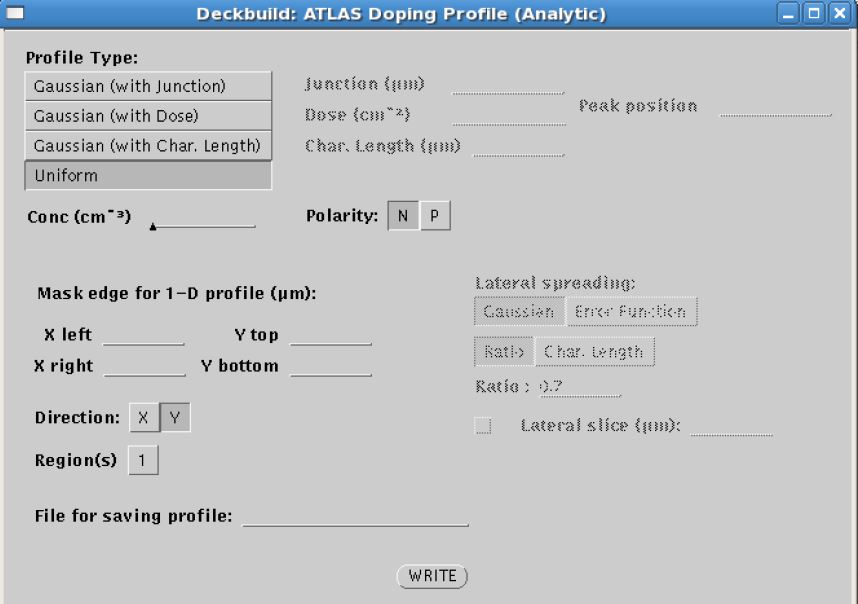
Select the profile type in this case we must select uniform Doping of N type material with Conc of 5e16.
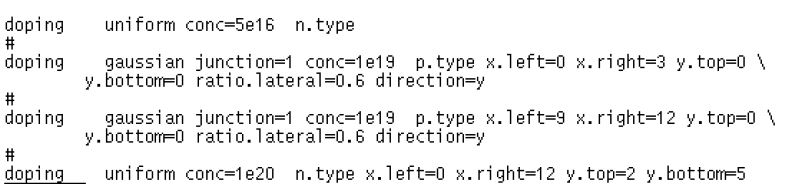
The following input line is generated in Deck build
doping n.type conc=5e16 uniform
Next we must define the junction by doping P-type material
Select Doping Profile as Gaussian (with junction) & Polarity of P type.
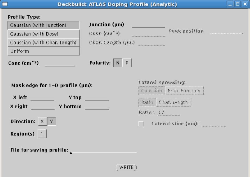
Concentration = 1e19 and define the doping coordinates x.left=0 x.right=3 y.top=0 y.bottom=0
Concentration= 1e19 and define the doping coordinates x.left=9 x.right=12 y.top=0 y.bottom=0
We need to perform the uniform doping of n-type polarity
Again right click on Commands…right click on Structure….right click on Doping….Click on Analytic and select the profile type as uniform doping of N-type with Concentration 1e20
Click on write button the following input deck appears on the Deckbuild
We need to save this structure file, this file will be used for the device characteristics simulation.
Right click on Commands…click on Solutions and then click on Save
Click the output file as Testdiode.str
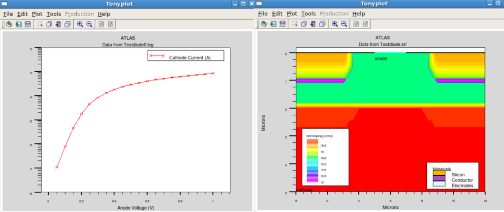
Now run the simulation, we will get the following Diode Structure.
Simulation of I-V Characteristic Curve using Silvaco Atlas
We will use the same device structure to simulate the diode device characteristics. We need to call our structure file which we had previously save as save outf=Testdiode.str
Mesh infile=Testdiode.str
Schottky Diode device characteristics simulation
For the device characteristics we must select the appropriate device model, these are specified using the MODELS and IMPACT statements.
Right click on Commands…right click on Models…Models( Right click on defaults select Bipolar instead of MOS)
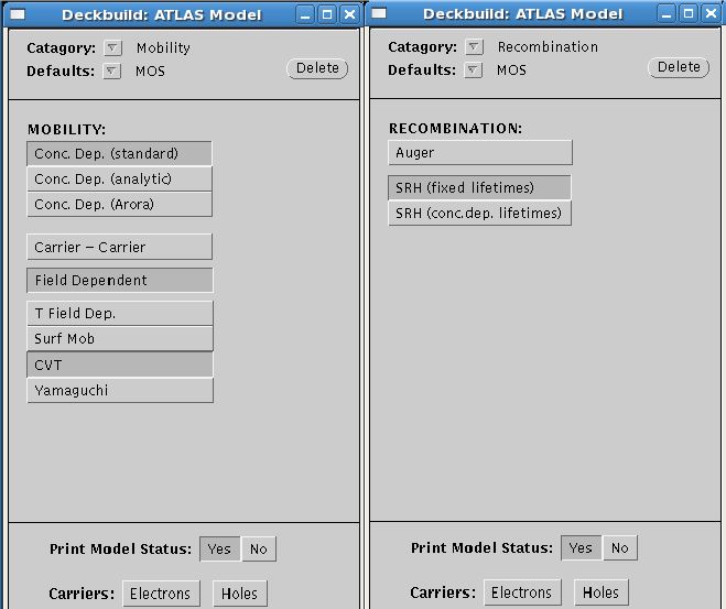
Atlas provides an easy method for selecting the correct models for various technologies. The MOS, BIP, PROGRAM, and ERASE parameters for the MODELS statement configure a basic set of mobility, recombination, carrier statistics, and tunneling models. The MOS and BIP parameters enable the models for MOSFET and bipolar devices, while PROGRAM and ERASE enable the models for programming and erasing programmable devices.
Click on write button the following input statement will appear on the Deckbuild window.
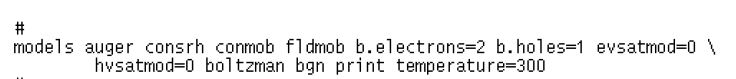
To define the appropriate model for Diode, define the following input statement on the Deckbuild window
Model Bipolar print
Choosing the Numerical Model
Numerical methods are given in the METHOD statements of the input file. Different combinations of models will require ATLAS to solve up to six equations. There are basically three types of solution techniques
1) Decoupled (GUMMEL)
2) Fully coupled (NEWTON)
3) BLOCK.
GUMMEL method will solve for each unknown in turn keeping the other variable constant, repeating the process until a stable solution is achieved. The NEWTON method solves the total system of unknowns together. The BLOCK methods will solve some equations fully coupled while others are decoupled.
The GUMMEL method is useful where system of equations is weakly coupled but has only linear convergence.
The Newton method is useful when the system of equations is strongly coupled and has quadratic convergence. NEWTON method may spend more time solving for quantities, which are essentially constant or weakly coupled. NEWTON also requires a more accurate initial guess to the problem to obtain convergence.
BLOCK method can provide for faster simulations times in these cases over NEWTON.
GUMMEL can provide better initial guess to the problems, so it is better to start the solution with a few GUMMEL iterations to generate better guess, then switch to NEWTON to complete the solution.
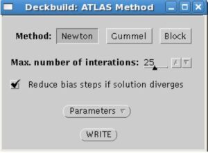
In this Silvaco tutorial we will use Newton method, where we also define the more accurate initial guess in order to obtain the Convergence.
We defined the Newton model by following input statement on the Deckbuild window
Method Newton
We can right click on commands, right click on solutions & click on Method, select method as Newton, select Max number of iterations, then click on Write
Obtaining solutions
Atlas can calculate DC, AC small signal and transient solutions. In this case we usually define the voltages on each of the electrodes in the device. Atlas then calculates the current through each electrode. In all simulations, the device starts with zero bias on all electrodes. Solutions are obtained by stepping the biases on electrodes from this initial equilibrium condition.
Right click on Commands…right click on Solutions…click on Solve
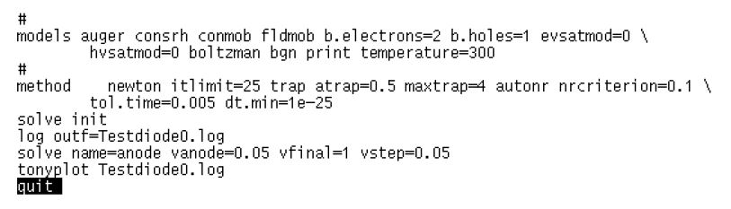
SOLVE INIT
Solve Vanode=0.05 Vstep=0.05 Vfinal=1 name=anode.
Now to plot the device structure and the device characteristics, type the following command on Deckbuild window.
The structure file which we saved as Testdiode.str
To plot the Diode structure.
Type the following command on Deckbuild.
tonyplot Testdiode.str
To save the I-V Characteristic Curve of the Diode, type the following command on the Deckbuild window.
log outf=Testdiode.log
tonyplot Testdiode.log
End of tutorial
If you require the Deckbuild file please drop a email.
Great job as always