
Modern world surrounded by sophisticated gadgets, without these gadgets, it is difficult to perform our day to day activities. Technology has made humans dependent on these gadgets, which are getting smaller and hitting the threshold limits. You would have experienced at least once in your lifetime, that your smartphone battery is about to exhaust, and you have just got minimal time to recharge your battery.
To overcome this scientists, and engineers are developing new material such as GaN, ZnO, and Ga2O3 to replace the Silicon material. Gallium nitride is shaping up to replace Silicon, and it is 1000 times more efficient in conducting electricity. You would have also felt your charger gets overheated, which is a waste of energy that has turned into heat.
Gallium nitride material has a wider bandgap and eliminates up to 90% power loss during power conversion. GaN power devices are heterojunction in nature, where the interface between two different semiconductors with dissimilar band gaps and the lattice mismatch must be small. An enormous lattice mismatch generates defects in the crystal lattice, which influences the electrical behavior of the device.
Wide bandgap semiconductors (bandgap> 3eV) such as SiC, GaN, ZnO, and Ga2O3 possess attractive characteristics and potential candidates for power device applications. Wide bandgap semiconductors have larger bandgap and higher breakdown than silicon material.
The below table provides the characteristics of various semiconductor material used in power device technology.
| Silicon | 4H-SiC | GaN | Ga203 | |
| Bandgap Energy(eV) | 1.12 | 3.25 | 3.4 | 4.5-4.9 |
| Dielectric constant | 11.8 | 9.7 | 9 | 10 |
| Breakdown field(MV/cm) | 1.5 | 4.9 | 2.3 | 0.25 |
| Thermal conductive | 1.5 | 4.9 | 2.3 | 0.25 |
| Electron mobility(cm²/Vs) | 1500 | 1000 | 1250 | 300 |
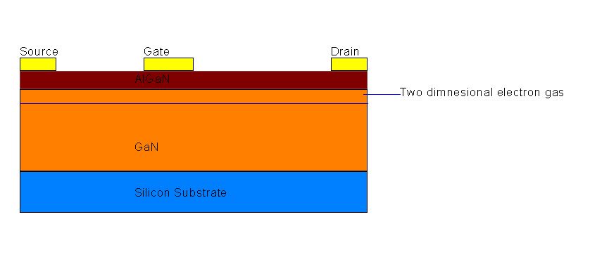
Working of GaN technology device
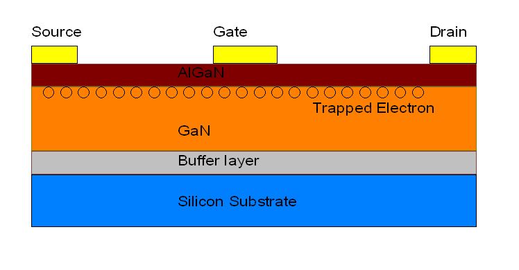
The working of a GaN technology power device is due to the high electron mobility in the two-dimensional electron gas between the GaN and the AlGaN layers. The two-dimensional electron gas caused due to the piezoelectric and polarization effect between the GaN and AlGaN. The concern for a GaN power device is the inherent reliability concern due to the electron trap, which causes crystal dislocation, blocks the drain current flow, and results in higher dynamic RDS (on) called as current collapse.
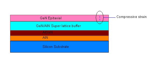
 The GaN epitaxial layer caused due to compressive strain due to the growing GaN on the Silicon wafer and to mitigate the crystal dislocation through the superlattice buffer that would reduce the crystal dislocations to a certain extent.
 Electron trapping can occur on the surface, and the bulk of GaN caused due to the crystal dislocation. Higher the electric field more the electrons trapped, which blocks the drain current flow and increases the RDS(on), as the resistance increases the device heats up and negatively impacts the reliability. RDS can be significantly higher than RDS (on) reported on the datasheet, the dynamic condition while the GaN device is being switched ON and OFF during high voltage. Higher the voltage and higher the electric field more the electrons are trapped.
JEDEC standard test for silicon powered devices is a static test condition, and it doesn’t cover dynamic conditions such as dynamic RDS (on). For a GaN-based device, we need to think beyond the standard JEDEC test method to determine the intrinsic reliability, HTOL test to ascertain the operating life of the product.
Factors which influence the reliability of the device
1) Thermal Stress
2) Dynamic RDS (on)
3) Field Data Simulation
For a GaN technology device, thermal stress leakage to be determined through the JEDEC standard static test. The current collapse condition impacts the reliability of the GaN technology device and occurs due to the trapped electrons when the high voltage is applied. To gauge the reliability under a dynamic condition would need testing beyond the JEDEC standard test.
GaN normally-on device, to turn into a normally-off device this can be done through enhancement-mode or cascode. One of the breakthroughs achieved in the GaN-based technology is by Panasonic based on the HD-GiT technology.
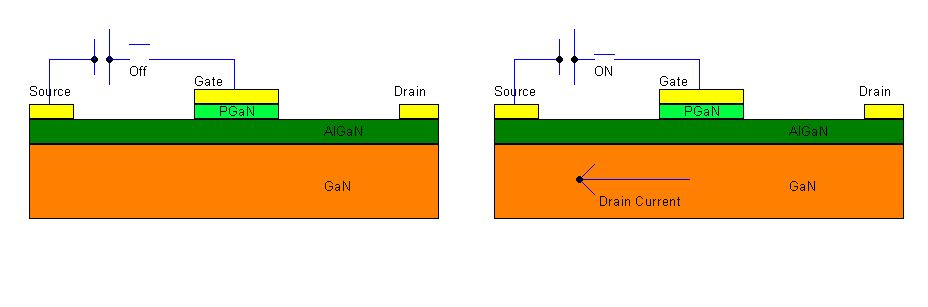 The P-layer diffused under the gate with a resistance connection, termed as GiT (Gate injection transistor), the P-layer lifts the potential at the channel, and the electron movement is blocked above the threshold voltage, and the current flow starts again. To minimize, the current collapse in the GaN-based device, by diffusing a second p-dope gate near the drain. The second gate automatically turns on during the switching period, and trapped electrons released by holes injected.
GaN devices, have no parasitic resistance and cannot create avalanche proof. X-GaN by Panasonic design with Vds breakdown voltage 900V, due to wide-bandgap and no longer necessary for avalanche proof technique that helps design engineers.
GaN based device has the advantages over Silicon-based
1) Higher Switching frequency and lower RDS (on)
2) Cheaper technology compared to SiC
3) High electron mobility of electrons in the channel
4) Higher breakdown voltage compared to silicon based power devices
Area of applications
1) GaN devices used for RF energy applications
2) Smaller AC adapters and consumer electronics goods in the future
3) Motor drives for E-Bikes
4) Electric vehicle charging station
 Image Credit: Pixabay