How to simulate operational amplifier using LTspice? Before that let us understand about Operational amplifier.
Without an Operational amplifier, we can never imagine the current gadget world. The contribution of the Operational amplifier is immense and find use in various technology. Most youths love to party during the weekend, and the question they come across, are you dancing tonight?
The answer depends on the ability of the Disco jockey. But how does the DJ controls the music and sound equipment at the nightclubs?
Ever thought about how the volume of the sound system controlled?
Then we must thank design engineers for inventing the operational amplifiers, which is the basic building block used to provide gain for audio systems and voltage regulator application.
Ideal Operational amplifier
The figure below shows an ideal op-amp, the input impedance is denoted, as Rin and does not allow any current to flow into it. Ideally, the op-amp input impedance must be infinite, and the output impedance of op-amp denoted as Ro.
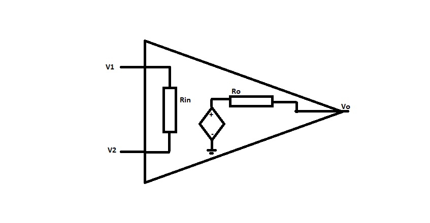
The Ro ensures that the output voltage of the op-amp remains the same for any value of load resistance connected. Ideally, the output impedance of op-amp must be zero. When we look into the open-loop voltage gain of an ideal op-amp, it is infinite. Then the difference between the two inputs can be applied by an ideal op-amp to infinity.
For an ideal op-amp, there is zero output voltage for zero input voltage then the input offset voltage is zero. An op-amp that starts to work as an amplifier at a particular frequency range is known as bandwidth. The bandwidth of an ideal op-amp is infinite, and it can amplify both DC and AC signals. The output voltage of op-amp changes immediately, with a change in the input voltage. If the output voltage doesn’t change immediately with the change in input, then there exists distortion in the output of the op-amp.
Let us understand the working of an operational amplifier using LTspice tools.
The fundamental building block of a two-stage operational amplifier consists of a differential amplifier in the first stage, followed by the gain stage, such as the common-source stage.
Operational amplifier using LTspice tools
Let’s start the circuit simulation of Operational amplifier using LTspice, to open a new schematic editor. Go to File, click on the new schematic.

Components required to design an Operational Amplifier are NMOS, PMOS, voltage source, wire, and ground. Now to place the NMOS and PMOS in the schematic, click on the component symbol, and select the component symbol popup from the list select the PMOS and NMOS.
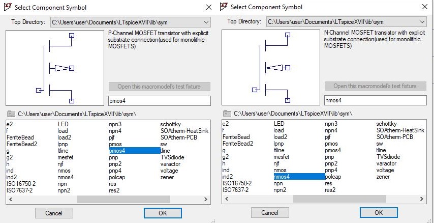
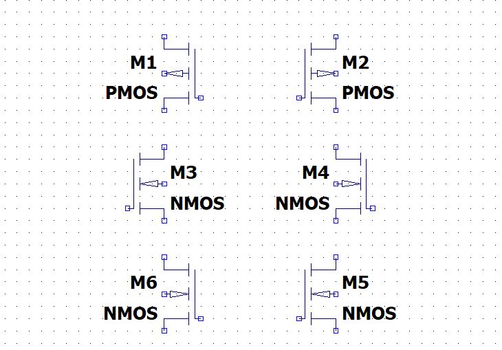
Now to mirror the PMOS device, Select M2 and use CTRL+E.
Place the PMOS and NMOS onto the schematic, the MOSFET terminal source connected to the bulk. You can use 4 terminal NMOS and PMOS device, which uses the symbol indicates substrate is p-type to n channel. As shown in the figure below, place all the PMOS and NMOS on the schematic window.
Connect the PMOS and NMOS using the wire, as shown in the image below.
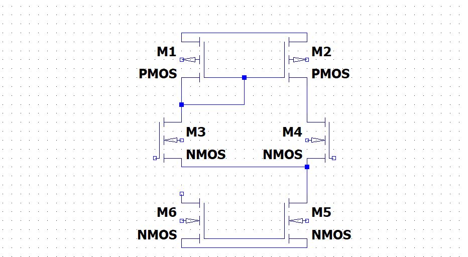
In this tutorial, we must define the VDD, V1, V2, IDC, and VSS as an input pin, as shown in fig below. Define the port type as an input or output. Click on Label net and define all the pins required for the operational amplifier circuit design.

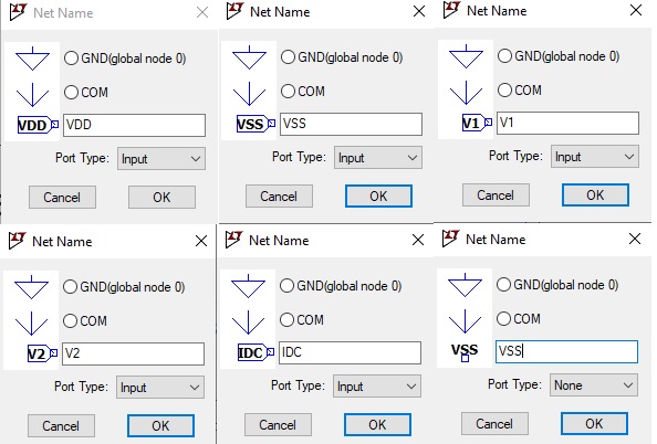
Place all the input and output pins on the schematic editor.
Connect all the pins and the MOSFET as shown in the figure below.
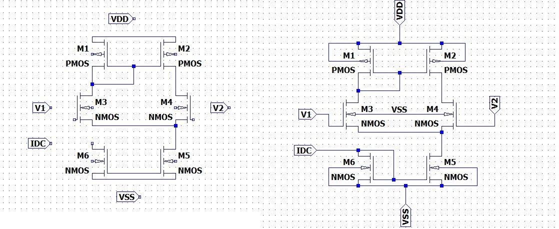
How to add model to LTspice
In this tutorial, we will use the BSIM model to predict the behavior of the Operational Amplifier.
For the latest BSIM model, you can download the following model from the link below.
https://drive.google.com/file/d/1uoeCOBqVdoeKjKEmSfaBuxtu3ru3YQrQ/view
In this example, we will use the Long Channel model. The BSIM model file must be in the same folder in which we save the schematic.
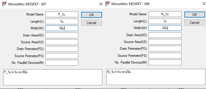
Right-click on the MOSFET and set the size of PMOS and NMOS as shown in the image below. Name the model as P_1u and N_1u as per the BSIM model file included in our simulation.
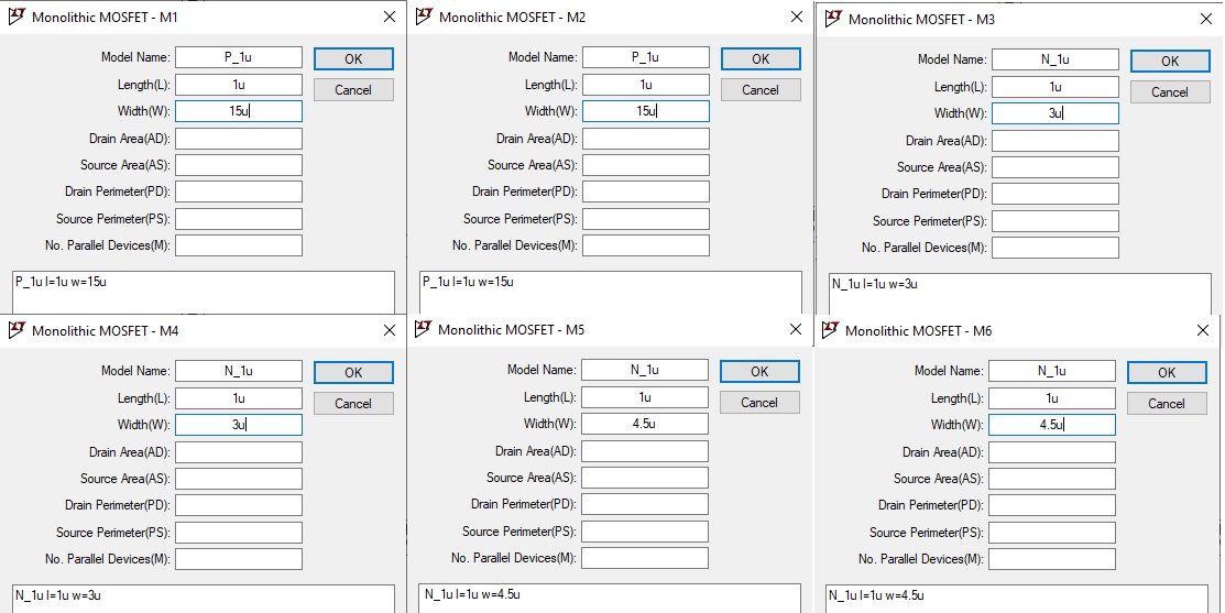
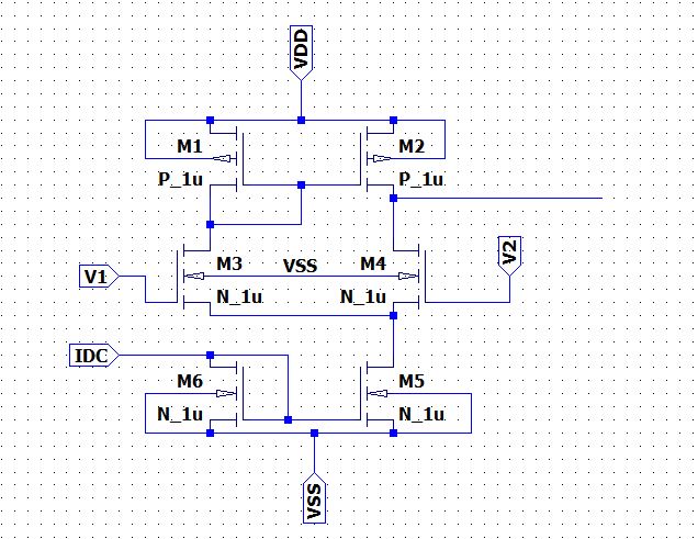
Now we must have a common source stage, click on components, and select a PMOS, NMOS, and capacitor. Place the component as shown in the schematic capture below, connect the output of the differential amplifier to the input of the common source stage.
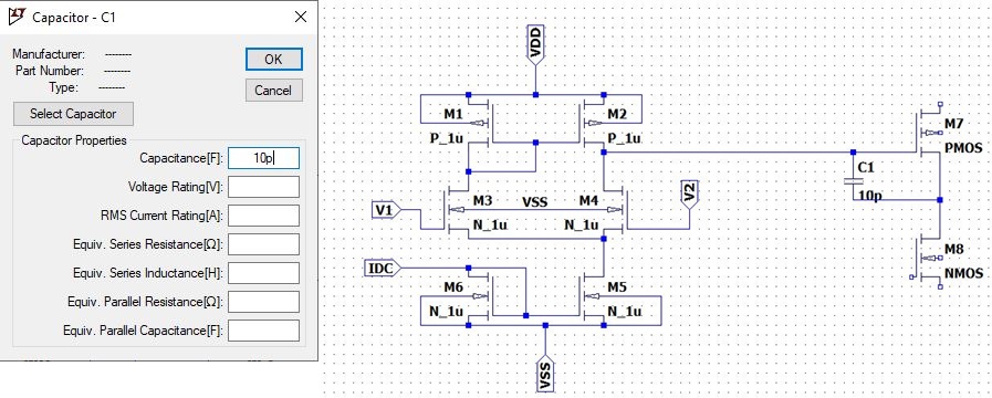
Right-click on the MOSFET and set the size of PMOS and NMOS as shown in the image below. Name the model as P_1u and N_1u as per the BSIM model file included in our simulation.
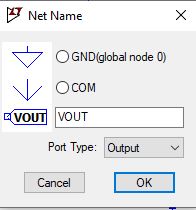
Click on label net, and define the label as VOUT and port type as output.
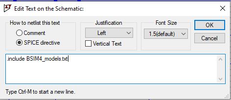
To include the BSIM model file, Go to edit and select SPICE Directive’S’ and then type .include BSIM4_model.txt.
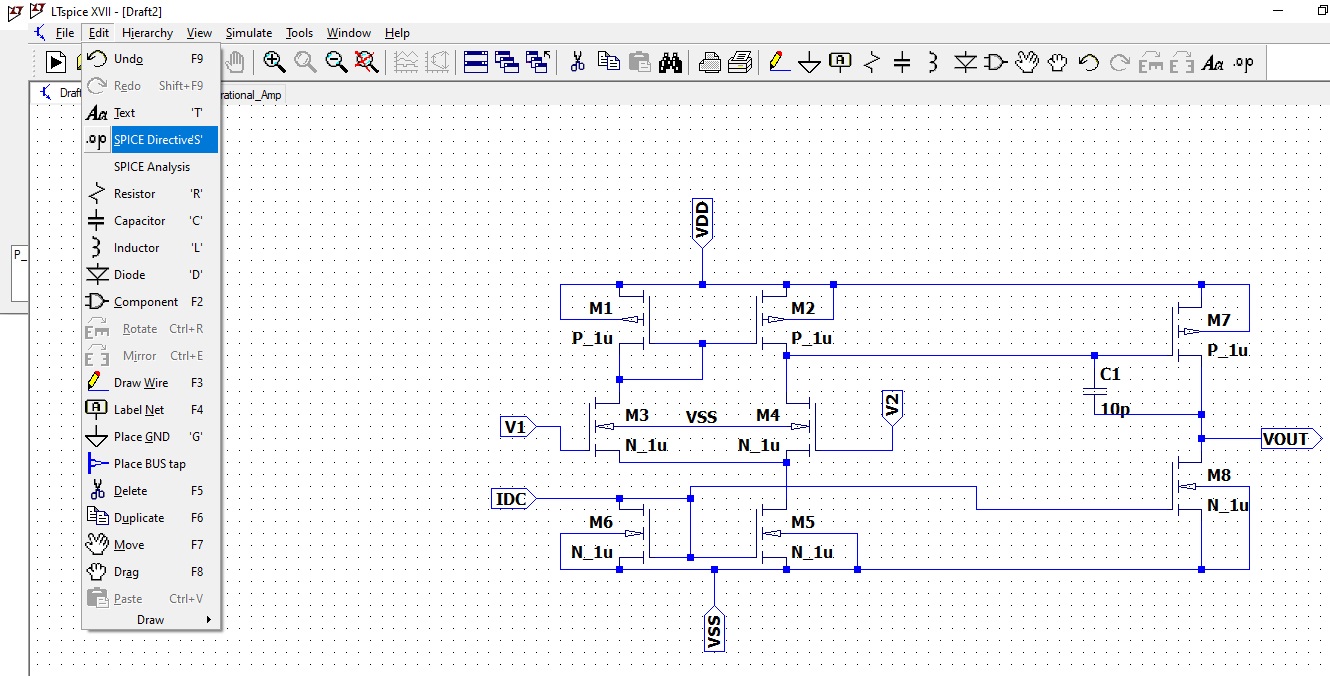
Edit text on schematic pop-up appears and type include BSIM_models.txt. Click ok the text appears on the schematic window.
How to create a symbol in LTspice?
The next section will guide you on how to create a symbol in LTspice. Click on Hierarchy and then select create a new symbol you will get a new schematic.
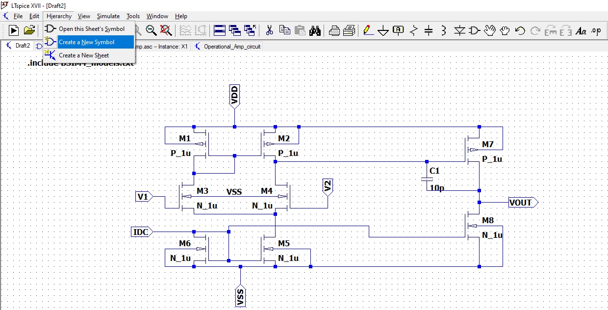
Save the symbol as OP_AMP symbol corresponds to the schematic which we had done earlier. Now click on the draw and then click on the line.

We will draw the Operational amplifier symbol and add the input and output pin to our symbol. Click on the edit and select add pin/port.
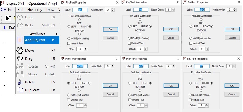
The pins are labeled as V1, V2, IDC, VDD, and VSS for the input terminal. The output terminal of the Operational amplifier is VOUT.
After placing all pins, the symbol is complete as shown in the image below.

Now to simulate the transient and DC analysis of the operational amplifier, click on the new schematic. Click on components and select the symbol which we had created OP_AMP. Place the symbol on the schematic, we must have a voltage source for VDD, VSS, V1, V2, IDC. Click on components and select the voltage and current source.
Double click on VDD, VSS, and IDC and define the value as shown in the table below.
| Voltage Source | Volts |
| VDD | 2.5V |
| VSS | -2.5V |
| V1 | DC offset-0V, Amplitude-5mV, Frequency-1 KHz |
| V2 | GND |
| IDC | 10u |
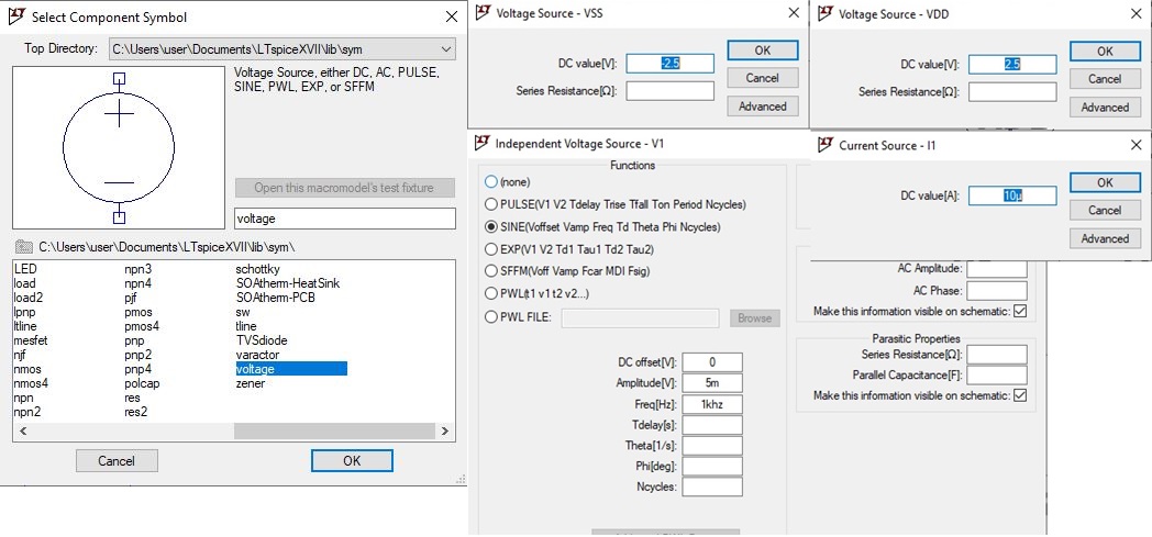
The first source of sweep will be V1, the start value to be -2.5, and the stop value as 2.5V with 0.1 volt increment.
Click on ok. The following syntax appears on the schematic window.
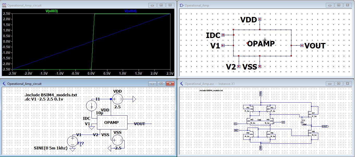
.dc V1 -2.5 2.5 0.1V
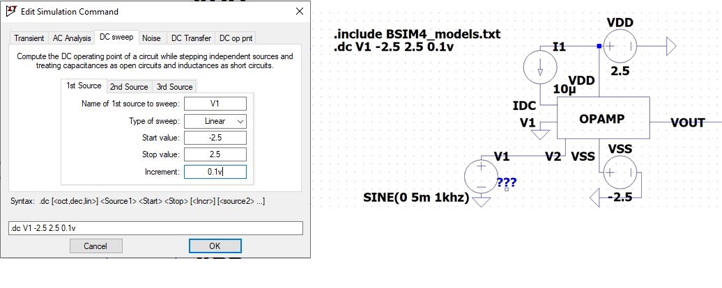
Click on run button, select the input V1 and VOUT.
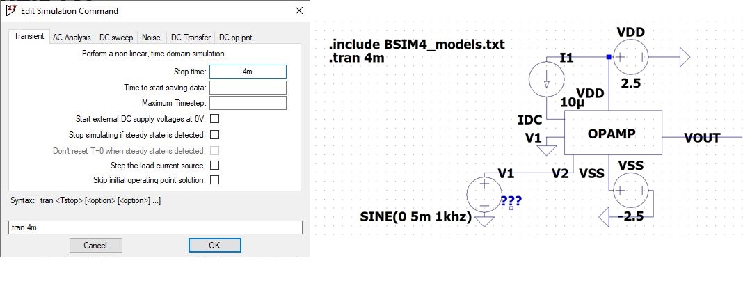
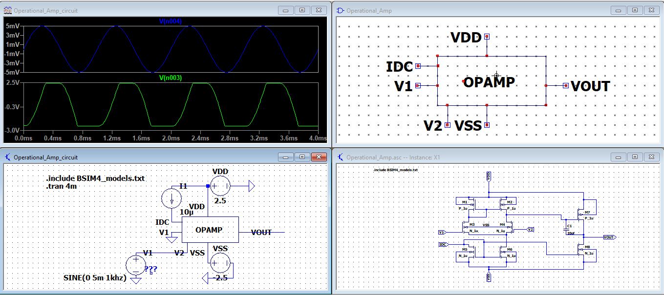
Right-click on to the .dc and change from DC sweep to transient analysis.
Click on run button, select the input V1 and VOUT.
End of the tutorial.