In this KiCad tutorial we will simulate a CMOS inverter circuit. We will use the AOS transistor model which we will add in the KiCad library. For any digital circuits CMOS inverter forms a basic building block.
In this KiCad tutorial we will perform the DC analysis of CMOS inverter, using AOS PMOS and NMOS devices from KiCad global library.
What is a CMOS Inverter?
When the input to the inverter is connected to ground, the output is pulled to VDD through the PMOS device (and NMOS device shuts off). When the input terminal is connected to VDD, the output is pulled to ground through the NMOS device (and PMOS device shuts off).
Let us start this KiCad tutorial. Open the KiCad tool and click on the file. Select the new project and save the name of the project as DC_Analysis_CMOSinv. Double click on the DC_Analysis_CMOSinv.sch and the schematic window appears. Now to place the components on the schematic window, on the right hand side click on the place symbol icon.
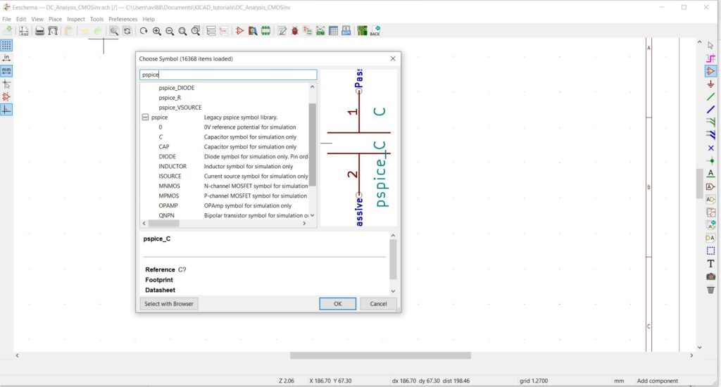
The Global KiCad Library loads, in the filter type pspice and from the list below select the N-channel Mosfet and P-Channel Mosfet and place this on the schematic window. Right click on the PMOS device select properties→ edit properties. A symbol properties pop-up appears, define the reference as M1 and click on edit spice model.
The Spice model editor pop-up appears, and provide the AOS model path and select the AON6667_P model and select the alternate model sequence as 1 2 3.
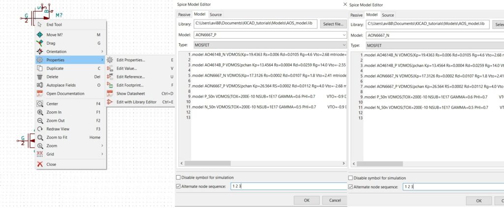
Follow the similar procedure for NMOS device and select the A0N6667_N model and select the alternate model sequence as 1 2 3.
Next we must place the global label, click on place global label and place the cursor on the schematic window. Now we require two input global labels Vin and VDD, and one output global label Vout.

KiCad tutorial on placing the voltage source
We must also place the voltage source for the Mosfet transistor and the input voltage to drive the CMOS inverter. On the right hand side click on the place symbol icon.
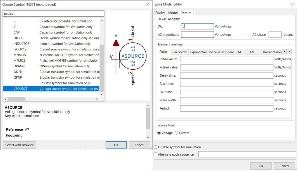
The Global KiCad Library loads, in the filter type pspice and from the list below select the VSOURCE, place two voltage sources. Now we must define the value for the following voltage sources. Right click on the voltage source select properties→ edit properties. A symbol properties pop-up appears, define the reference as VDD and click on edit spice model. Select the source as DC analysis and define the DC voltage as 5 volts, similarly define the same for the Vin voltage source.
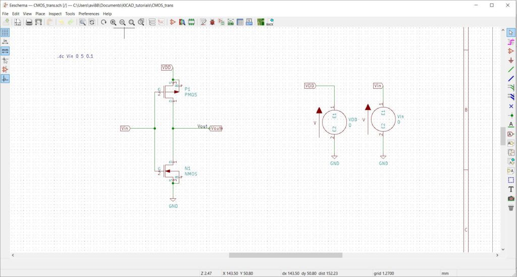
Next we must place the ground connection for the voltage source, and for the CMOS inverter circuit. On the right hand side click on the place power port, and place the cursor on the schematic window. The KiCad library pops-up, in the filter type GND, and select the ground and place it on the schematic. To duplicate the GND, right click on ground, and select duplicate and place the ground accordingly. We must also place the global label VDD, and Vin near the voltage source. Now connect the components using wire, on the right hand side click on the wire. Make the connections accordingly as shown in the figure below.
KiCad tutorial on how to define the spice input
Now to simulate the DC analysis of a CMOS inverter, we must define the input statement which ngspice understands.
Click on place and select the graphic text, the text properties pop-up box appears.
Type .dc Vin 0 5 0.1
The input voltage drives from 0 to 5 volts with 0.1 volts incremental increase.
To run the simulation, click on tools and select simulation.
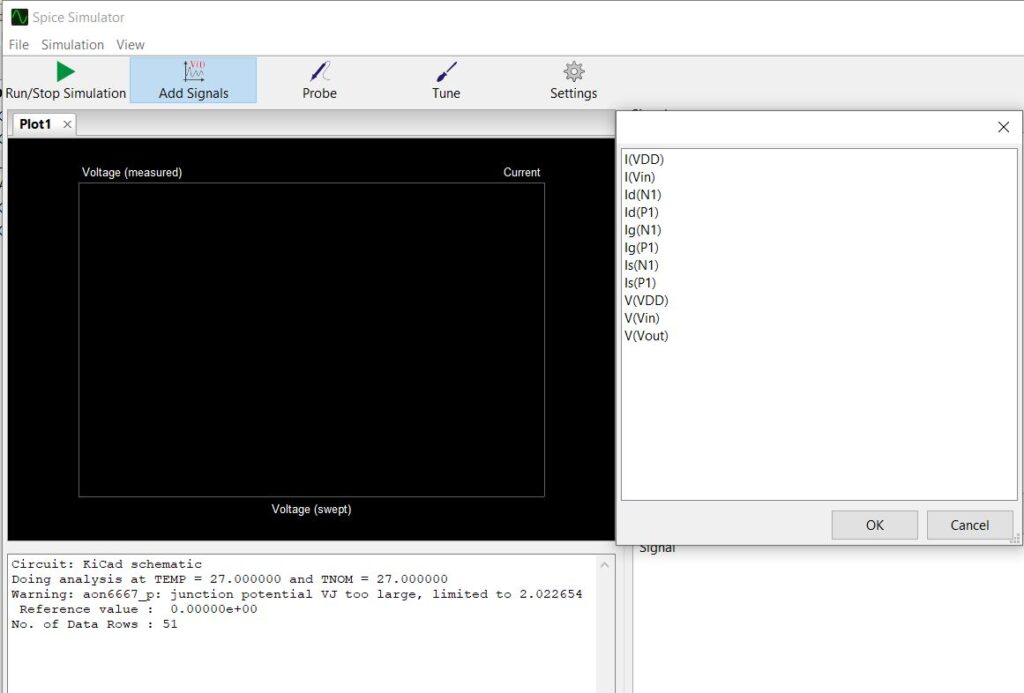
Click on Run/Stop simulation button, next click on add signal and select Vin and Vout.
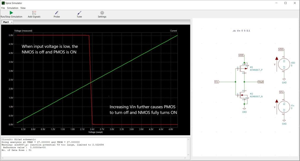
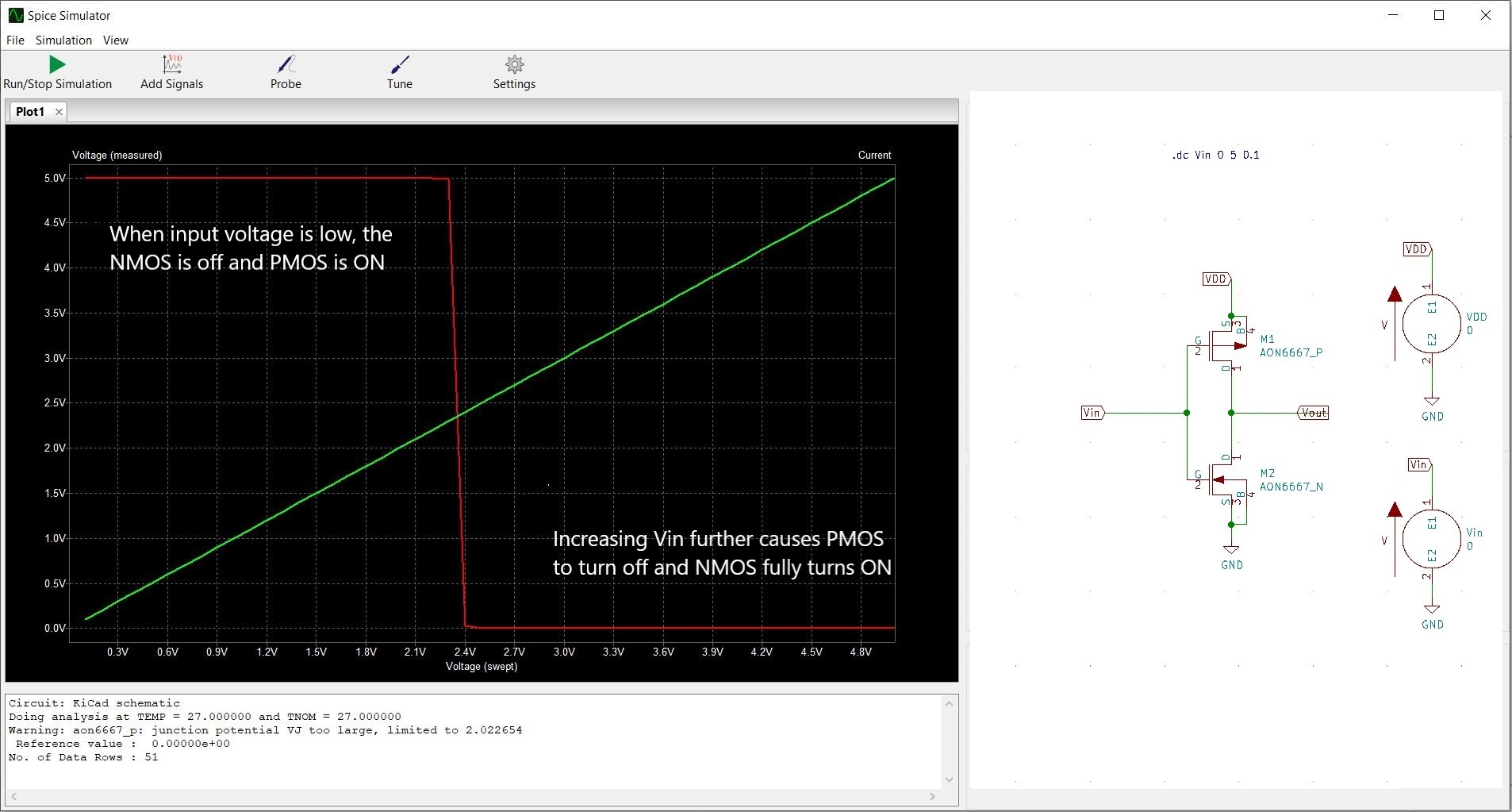
From the DC analysis we can note that, when input voltage is low. The NMOS device is off and the PMOS device is on. When Vin increases, both PMOS and NMOS turn on, on further increase in Vin PMOS turns off and NMOS turns on.
End of tutorial
1 thought on “KiCad tutorial on CMOS inverter circuit simulation”