How does an Gated SR latch work?
A Gated SR latch is always desirable to prevent input activation signals affecting the state of the latch immediately. But rather to have effect occur at some desirable time. In such scenario engineers consider Gated SR .
Gated SR latch consists of SR latch along with two additional NAND gates and a control input C. The enable input C determines when the S and R inputs become effective.
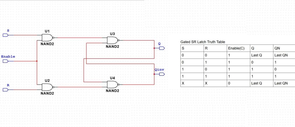 Logic Diagram and Function table
As long as the enable input is zero, the output of the NAND gate A and B are high, and the latch is in its current stable state.
Any changes on the SR line are blocked, and the output latched to the present state, and the latch is disabled.
When the enable signal is 1, the latch is enabled. If the input S and R are equal to zero, the latch is in the current stable state.
When the input at the R terminal is equal to 1 and S is equal to zero, the latch is being reset.
If the input to R returns to zero, then the latch returns to its present state as described in the row below.
Gated SR Latch Truth Table
| S | R | Enable(C) | Q | QN |
| 0 | 0 | 1 | Last Q | Last QN |
| 0 | 1 | 1 | 0 | 1 |
| 1 | 0 | 1 | 1 | 0 |
| 1 | 1 | 1 | 1 | 1 |
| X | X | 0 | Last Q | Last QN |
When the input S is high then the latch becomes set regardless of the present state. If the input applied to both the S and R is high and the signal to enable is 1 then the latch enters into an unpredictable state.
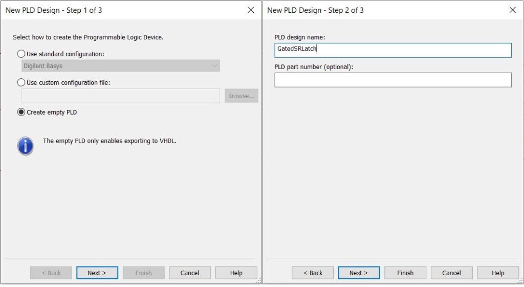
Design and simulation using multisim.
Let us start the design and simulation of the Gated SR latch using the multisim tool. Click on new and select PLD design and click create. Select create empty PLD and click next and type the PLD design name and click on finish.
 PLD Design Multisim
Now click on the place logic gate and select a two-input NAND gate and place the NAND gates on the schematic window.
Connect the output of NAND gate three to one of the inputs of NAND gate four, and the connect output of NAND gate 4 to the input of NAND gate 3.
Connect the output of NAND gate 1 to the input of NAND gate 3 and the output of NAND gate 2 to the input of NAND gate 4.
Next, click on the input connector and place two inputs S and R.
For a gated SR latch, place an enabled input C. Connect the input connectors to the NAND gates and rename the input connectors as S and R.
Now place an output connector, click on the output connector and place this on the NAND gate output 3 and 4.
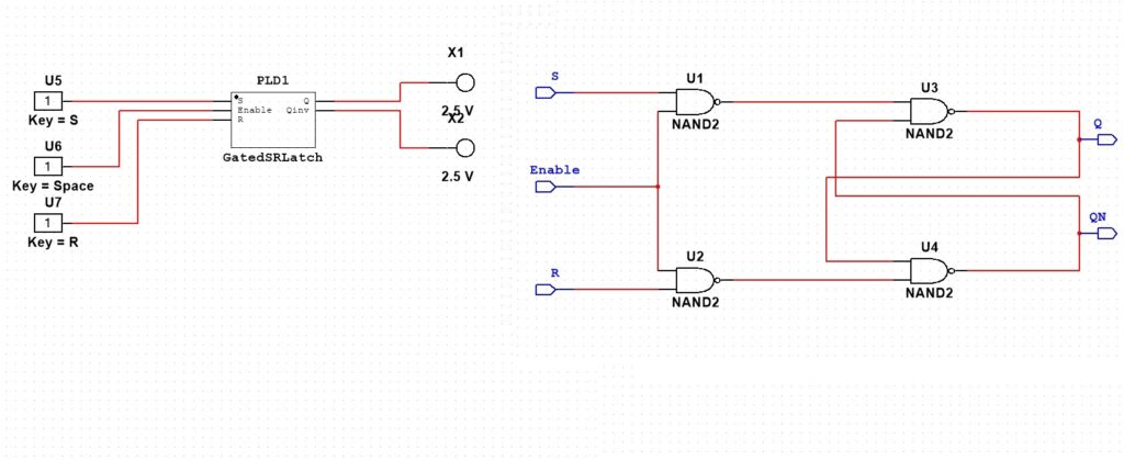
Gated SR Latch hierarchical block
This helps in the simulation of the low and high signals. To determine the output or the working of the gated SR latch we must place a probe.
To change the value of the toggle click on the interactive digital constant.
You can realize the operation of the Gated SR latch accordingly.
End of tutorial